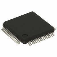
ST72F321BR9T6 STMicroelectronics, ST72F321BR9T6 Datasheet - Page 106

ST72F321BR9T6
Manufacturer Part Number
ST72F321BR9T6
Description
MCU 8BIT 60KB FLASH/ROM 64-LQFP
Manufacturer
STMicroelectronics
Series
ST7r
Datasheet
1.ST72F321BK6T6.pdf
(187 pages)
Specifications of ST72F321BR9T6
Core Processor
ST7
Core Size
8-Bit
Speed
8MHz
Connectivity
I²C, SCI, SPI
Peripherals
LVD, POR, PWM, WDT
Number Of I /o
48
Program Memory Size
60KB (60K x 8)
Program Memory Type
FLASH
Ram Size
2K x 8
Voltage - Supply (vcc/vdd)
3.8 V ~ 5.5 V
Data Converters
A/D 16x10b
Oscillator Type
Internal
Operating Temperature
-40°C ~ 85°C
Package / Case
64-LQFP
Processor Series
ST72F3x
Core
ST7
Data Bus Width
8 bit
Data Ram Size
2 KB
Interface Type
I2C, SCI, SPI
Maximum Clock Frequency
8 MHz
Number Of Programmable I/os
48
Number Of Timers
2
Maximum Operating Temperature
+ 85 C
Mounting Style
SMD/SMT
Development Tools By Supplier
ST7232X-EVAL, ST7232X-SK/RAIS, ST72321B-D/RAIS, ST7MDT20-DVP3, STX-RLINK
Minimum Operating Temperature
- 40 C
On-chip Adc
10 bit, 16 Channel
Cpu Family
ST7
Device Core Size
8b
Frequency (max)
8MHz
Total Internal Ram Size
2KB
# I/os (max)
48
Number Of Timers - General Purpose
2
Operating Supply Voltage (typ)
5V
Operating Supply Voltage (max)
5.5V
Operating Supply Voltage (min)
3.8V
Instruction Set Architecture
CISC
Operating Temp Range
-40C to 85C
Operating Temperature Classification
Industrial
Mounting
Surface Mount
Pin Count
64
Package Type
LQFP
For Use With
497-5046 - KIT TOOL FOR ST7/UPSD/STR7 MCU
Lead Free Status / RoHS Status
Lead free / RoHS Compliant
Eeprom Size
-
Lead Free Status / Rohs Status
Details
Other names
497-5586
Available stocks
Company
Part Number
Manufacturer
Quantity
Price
Company:
Part Number:
ST72F321BR9T6
Manufacturer:
STMicroelectronics
Quantity:
10 000
ST72321BRx, ST72321BARx ST72321BJx, ST72321BKx
SERIAL COMMUNICATIONS INTERFACE (Cont’d)
10.6.4.7 Parity Control
Parity control (generation of parity bit in transmis-
sion and parity checking in reception) can be ena-
bled by setting the PCE bit in the SCICR1 register.
Depending on the frame length defined by the M
bit, the possible SCI frame formats are as listed in
Table
Table 21. Frame Formats
Legend: SB = Start Bit, STB = Stop Bit,
PB = Parity Bit
Note: In case of wake up by an address mark, the
MSB bit of the data is taken into account and not
the parity bit
Even parity: the parity bit is calculated to obtain
an even number of “1s” inside the frame made of
the 7 or 8 LSB bits (depending on whether M is
equal to 0 or 1) and the parity bit.
Example: data = 00110101; 4 bits set => parity bit
is 0 if even parity is selected (PS bit = 0).
Odd parity: the parity bit is calculated to obtain an
odd number of “1s” inside the frame made of the 7
or 8 LSB bits (depending on whether M is equal to
0 or 1) and the parity bit.
Example: data = 00110101; 4 bits set => parity bit
is 1 if odd parity is selected (PS bit = 1).
Transmission mode: If the PCE bit is set then the
MSB bit of the data written in the data register is
not transmitted but is changed by the parity bit.
Reception mode: If the PCE bit is set then the in-
terface checks if the received data byte has an
106/187
M bit
0
0
1
1
1.
PCE bit
0
1
0
1
| SB | 7-bit data | PB | STB |
| SB | 8-bit data PB | STB |
| SB | 8 bit data | STB |
| SB | 9-bit data | STB |
SCI frame
even number of “1s” if even parity is selected
(PS = 0) or an odd number of “1s” if odd parity is
selected (PS = 1). If the parity check fails, the PE
flag is set in the SCISR register and an interrupt is
generated if PIE is set in the SCICR1 register.
10.6.4.8 SCI Clock Tolerance
During reception, each bit is sampled 16 times.
The majority of the 8th, 9th and 10th samples is
considered as the bit value. For a valid bit detec-
tion, all the three samples should have the same
value otherwise the noise flag (NF) is set. For ex-
ample: If the 8th, 9th and 10th samples are 0, 1
and 1 respectively, then the bit value is “1”, but the
Noise Flag bit is set because the three samples
values are not the same.
Consequently, the bit length must be long enough
so that the 8th, 9th and 10th samples have the de-
sired bit value. This means the clock frequency
should not vary more than 6/16 (37.5%) within one
bit. The sampling clock is resynchronized at each
start bit, so that when receiving 10 bits (one start
bit, 1 data byte, 1 stop bit), the clock deviation
must not exceed 3.75%.
Note: The internal sampling clock of the microcon-
troller samples the pin value on every falling edge.
Therefore, the internal sampling clock and the time
the application expects the sampling to take place
may be out of sync. For example: If the baud rate
is 15.625 Kbaud (bit length is 64µs), then the 8th,
9th and 10th samples are at 28µs, 32µs and 36µs
respectively (the first sample starting ideally at
0µs). But if the falling edge of the internal clock oc-
curs just before the pin value changes, the sam-
ples would then be out of sync by ~4us. This
means the entire bit length must be at least 40µs
(36µs for the 10th sample + 4µs for synchroniza-
tion with the internal sampling clock).


