ST72F321BR9T6 STMicroelectronics, ST72F321BR9T6 Datasheet - Page 96
ST72F321BR9T6
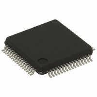
Manufacturer Part Number
ST72F321BR9T6
Description
MCU 8BIT 60KB FLASH/ROM 64-LQFP
Manufacturer
STMicroelectronics
Series
ST7r
Datasheet
1.ST72F321BK6T6.pdf
(187 pages)
Specifications of ST72F321BR9T6
Core Processor
ST7
Core Size
8-Bit
Speed
8MHz
Connectivity
I²C, SCI, SPI
Peripherals
LVD, POR, PWM, WDT
Number Of I /o
48
Program Memory Size
60KB (60K x 8)
Program Memory Type
FLASH
Ram Size
2K x 8
Voltage - Supply (vcc/vdd)
3.8 V ~ 5.5 V
Data Converters
A/D 16x10b
Oscillator Type
Internal
Operating Temperature
-40°C ~ 85°C
Package / Case
64-LQFP
Processor Series
ST72F3x
Core
ST7
Data Bus Width
8 bit
Data Ram Size
2 KB
Interface Type
I2C, SCI, SPI
Maximum Clock Frequency
8 MHz
Number Of Programmable I/os
48
Number Of Timers
2
Maximum Operating Temperature
+ 85 C
Mounting Style
SMD/SMT
Development Tools By Supplier
ST7232X-EVAL, ST7232X-SK/RAIS, ST72321B-D/RAIS, ST7MDT20-DVP3, STX-RLINK
Minimum Operating Temperature
- 40 C
On-chip Adc
10 bit, 16 Channel
Cpu Family
ST7
Device Core Size
8b
Frequency (max)
8MHz
Total Internal Ram Size
2KB
# I/os (max)
48
Number Of Timers - General Purpose
2
Operating Supply Voltage (typ)
5V
Operating Supply Voltage (max)
5.5V
Operating Supply Voltage (min)
3.8V
Instruction Set Architecture
CISC
Operating Temp Range
-40C to 85C
Operating Temperature Classification
Industrial
Mounting
Surface Mount
Pin Count
64
Package Type
LQFP
For Use With
497-5046 - KIT TOOL FOR ST7/UPSD/STR7 MCU
Lead Free Status / RoHS Status
Lead free / RoHS Compliant
Eeprom Size
-
Lead Free Status / Rohs Status
Details
Other names
497-5586
Available stocks
Company
Part Number
Manufacturer
Quantity
Price

Company:
Part Number:
ST72F321BR9T6
Manufacturer:
STMicroelectronics
Quantity:
10 000


ST72321BRx, ST72321BARx ST72321BJx, ST72321BKx
SERIAL PERIPHERAL INTERFACE (Cont’d)
10.5.8 Register Description
CONTROL REGISTER (SPICR)
Read/Write
Reset Value: 0000 xxxx (0xh)
Bit 7 = SPIE Serial Peripheral Interrupt Enable.
This bit is set and cleared by software.
0: Interrupt is inhibited
1: An SPI interrupt is generated whenever
Bit 6 = SPE Serial Peripheral Output Enable.
This bit is set and cleared by software. It is also
cleared by hardware when, in master mode, SS=0
(see
(MODF)). The SPE bit is cleared by reset, so the
SPI peripheral is not initially connected to the ex-
ternal pins.
0: I/O pins free for general purpose I/O
1: SPI I/O pin alternate functions enabled
Bit 5 = SPR2 Divider Enable.
This bit is set and cleared by software and is
cleared by reset. It is used with the SPR[1:0] bits to
set the baud rate. Refer to
mode SCK
0: Divider by 2 enabled
1: Divider by 2 disabled
Note: This bit has no effect in slave mode.
Bit 4 = MSTR Master Mode.
This bit is set and cleared by software. It is also
cleared by hardware when, in master mode, SS=0
(see
(MODF)).
0: Slave mode
1: Master mode. The function of the SCK pin
96/187
SPIE SPE
SPIF=1, MODF=1 or OVR=1 in the SPICSR
register
changes from an input to an output and the func-
tions of the MISO and MOSI pins are reversed.
7
Section
Section
Frequency.
SPR2
10.5.5.1
10.5.5.1
MSTR
CPOL
Master
Master
Table 19 SPI Master
CPHA
Mode
Mode
SPR1
SPR0
Fault
Fault
0
Bit 3 = CPOL Clock Polarity.
This bit is set and cleared by software. This bit de-
termines the idle state of the serial Clock. The
CPOL bit affects both the master and slave
modes.
0: SCK pin has a low level idle state
1: SCK pin has a high level idle state
Note: If CPOL is changed at the communication
byte boundaries, the SPI must be disabled by re-
setting the SPE bit.
Bit 2 = CPHA Clock Phase.
This bit is set and cleared by software.
0: The first clock transition is the first data capture
1: The second clock transition is the first capture
Note: The slave must have the same CPOL and
CPHA settings as the master.
Bits 1:0 = SPR[1:0] Serial Clock Frequency.
These bits are set and cleared by software. Used
with the SPR2 bit, they select the baud rate of the
SPI serial clock SCK output by the SPI in master
mode.
Note: These 2 bits have no effect in slave mode.
Table 19. SPI Master mode SCK Frequency
edge.
edge.
Serial Clock
f
f
f
f
CPU
f
f
CPU
CPU
CPU
CPU
CPU
/128
/16
/32
/64
/4
/8
SPR2
1
0
0
1
0
0
SPR1
0
0
0
1
1
1
SPR0
0
0
1
0
0
1
Related parts for ST72F321BR9T6
Image
Part Number
Description
Manufacturer
Datasheet
Request
R

Part Number:
Description:
64/44-PIN 8-BIT MCU WITH 32 TO 60K FLASH/ROM, ADC, FIVE TIMERS, SPI, SCI, I2C INTERFACE
Manufacturer:
STMICROELECTRONICS [STMicroelectronics]
Datasheet:

Part Number:
Description:
STMicroelectronics [RIPPLE-CARRY BINARY COUNTER/DIVIDERS]
Manufacturer:
STMicroelectronics
Datasheet:
Part Number:
Description:
STMicroelectronics [LIQUID-CRYSTAL DISPLAY DRIVERS]
Manufacturer:
STMicroelectronics
Datasheet:

Part Number:
Description:
BOARD EVAL FOR MEMS SENSORS
Manufacturer:
STMicroelectronics
Datasheet:
Part Number:
Description:
NPN TRANSISTOR POWER MODULE
Manufacturer:
STMicroelectronics
Datasheet:
Part Number:
Description:
TURBOSWITCH ULTRA-FAST HIGH VOLTAGE DIODE
Manufacturer:
STMicroelectronics
Datasheet:
Part Number:
Description:
Manufacturer:
STMicroelectronics
Datasheet:
Part Number:
Description:
DIODE / SCR MODULE
Manufacturer:
STMicroelectronics
Datasheet:
Part Number:
Description:
DIODE / SCR MODULE
Manufacturer:
STMicroelectronics
Datasheet:
Part Number:
Description:
Search -----> STE16N100
Manufacturer:
STMicroelectronics
Datasheet:
Part Number:
Description:
Search ---> STE53NA50
Manufacturer:
STMicroelectronics
Datasheet:
Part Number:
Description:
NPN Transistor Power Module
Manufacturer:
STMicroelectronics
Datasheet: