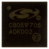
C8051F705-GM Silicon Laboratories Inc, C8051F705-GM Datasheet - Page 280

C8051F705-GM
Manufacturer Part Number
C8051F705-GM
Description
IC 8051 MCU 15K FLASH 48-QFN
Manufacturer
Silicon Laboratories Inc
Series
C8051F70xr
Specifications of C8051F705-GM
Core Processor
8051
Core Size
8-Bit
Speed
25MHz
Connectivity
SMBus (2-Wire/I²C), SPI, UART/USART
Peripherals
Cap Sense, POR, PWM, WDT
Number Of I /o
39
Program Memory Size
15KB (15K x 8)
Program Memory Type
FLASH
Eeprom Size
32 x 8
Ram Size
512 x 8
Voltage - Supply (vcc/vdd)
1.8 V ~ 3.6 V
Oscillator Type
Internal
Operating Temperature
-40°C ~ 85°C
Package / Case
48-QFN
Processor Series
C8051F7x
Core
8051
Data Bus Width
8 bit
Data Ram Size
512 B
Interface Type
I2C, SMBus, SPI, UART
Maximum Clock Frequency
25 MHz
Number Of Programmable I/os
39
Number Of Timers
4
Maximum Operating Temperature
+ 85 C
Mounting Style
SMD/SMT
3rd Party Development Tools
PK51, CA51, A51, ULINK2
Development Tools By Supplier
C8051F700DK
Minimum Operating Temperature
- 40 C
Height
0.95 mm
Length
7 mm
Supply Voltage (max)
1.9 V, 3.6 V
Supply Voltage (min)
1.7 V, 1.8 V
Width
7 mm
For Use With
336-1635 - DEV KIT FOR C8051F700
Lead Free Status / RoHS Status
Lead free / RoHS Compliant
Data Converters
-
Lead Free Status / Rohs Status
Details
Other names
336-1612-5
Available stocks
Company
Part Number
Manufacturer
Quantity
Price
Company:
Part Number:
C8051F705-GM
Manufacturer:
Silicon Laboratories Inc
Quantity:
135
- Current page: 280 of 306
- Download datasheet (2Mb)
C8051F70x/71x
33.3.3. Comparator 0 Capture Mode
The capture mode in Timer 3 allows Comparator 0 rising edges to be captured with the timer clocking from
the system clock or the system clock divided by 12. Timer 3 capture mode is enabled by setting TF3CEN
to 1 and T3SPLIT to 0.
When capture mode is enabled, a capture event will be generated on every Comparator 0 rising edge.
When the capture event occurs, the contents of Timer 3 (TMR3H:TMR3L) are loaded into the Timer 3
reload registers (TMR3RLH:TMR3RLL) and the TF3H flag is set (triggering an interrupt if Timer 3 inter-
rupts are enabled). By recording the difference between two successive timer capture values, the
Comparator 0 period can be determined with respect to the Timer 3 clock. The Timer 3 clock should be
much faster than the capture clock to achieve an accurate reading.
This mode allows software to determine the time between consecutive Comparator 0 rising edges, which
can be used for detecting changes in the capacitance of a capacitive switch, or measuring the frequency of
a low-level analog signal.
280
External Clock / 8
Comparator 0
SYSCLK / 12
SYSCLK
Output
T3XCLK
0
1
Figure 33.9. Timer 3 Capture Mode Block Diagram
T
M
H
3
M
T
3
L
0
1
CKCON
M
H
T
2
T
M
2
L
M
T
1
TF3CEN
M
T
0
S
C
A
1
TR3
S
C
A
0
Capture
Rev. 1.0
TCLK
TMR3RLL TMR3RLH
TMR3L
TMR3H
TF3CEN
T3SPLIT
TF3LEN
T3XCLK
TF3H
TF3L
TR3
Interrupt
Related parts for C8051F705-GM
Image
Part Number
Description
Manufacturer
Datasheet
Request
R
Part Number:
Description:
SMD/C°/SINGLE-ENDED OUTPUT SILICON OSCILLATOR
Manufacturer:
Silicon Laboratories Inc
Part Number:
Description:
Manufacturer:
Silicon Laboratories Inc
Datasheet:
Part Number:
Description:
N/A N/A/SI4010 AES KEYFOB DEMO WITH LCD RX
Manufacturer:
Silicon Laboratories Inc
Datasheet:
Part Number:
Description:
N/A N/A/SI4010 SIMPLIFIED KEY FOB DEMO WITH LED RX
Manufacturer:
Silicon Laboratories Inc
Datasheet:
Part Number:
Description:
N/A/-40 TO 85 OC/EZLINK MODULE; F930/4432 HIGH BAND (REV E/B1)
Manufacturer:
Silicon Laboratories Inc
Part Number:
Description:
EZLink Module; F930/4432 Low Band (rev e/B1)
Manufacturer:
Silicon Laboratories Inc
Part Number:
Description:
I°/4460 10 DBM RADIO TEST CARD 434 MHZ
Manufacturer:
Silicon Laboratories Inc
Part Number:
Description:
I°/4461 14 DBM RADIO TEST CARD 868 MHZ
Manufacturer:
Silicon Laboratories Inc
Part Number:
Description:
I°/4463 20 DBM RFSWITCH RADIO TEST CARD 460 MHZ
Manufacturer:
Silicon Laboratories Inc
Part Number:
Description:
I°/4463 20 DBM RADIO TEST CARD 868 MHZ
Manufacturer:
Silicon Laboratories Inc
Part Number:
Description:
I°/4463 27 DBM RADIO TEST CARD 868 MHZ
Manufacturer:
Silicon Laboratories Inc
Part Number:
Description:
I°/4463 SKYWORKS 30 DBM RADIO TEST CARD 915 MHZ
Manufacturer:
Silicon Laboratories Inc
Part Number:
Description:
N/A N/A/-40 TO 85 OC/4463 RFMD 30 DBM RADIO TEST CARD 915 MHZ
Manufacturer:
Silicon Laboratories Inc
Part Number:
Description:
I°/4463 20 DBM RADIO TEST CARD 169 MHZ
Manufacturer:
Silicon Laboratories Inc


