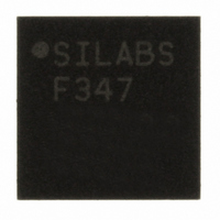
C8051F347-GM Silicon Laboratories Inc, C8051F347-GM Datasheet - Page 180

C8051F347-GM
Manufacturer Part Number
C8051F347-GM
Description
IC 8051 MCU 32K FLASH MEM 32-QFN
Manufacturer
Silicon Laboratories Inc
Series
C8051F34xr
Datasheet
1.C8051F349-GQ.pdf
(276 pages)
Specifications of C8051F347-GM
Program Memory Type
FLASH
Program Memory Size
32KB (32K x 8)
Package / Case
32-QFN
Core Processor
8051
Core Size
8-Bit
Speed
25MHz
Connectivity
SMBus (2-Wire/I²C), SPI, UART/USART, USB
Peripherals
Brown-out Detect/Reset, POR, PWM, Temp Sensor, WDT
Number Of I /o
25
Ram Size
2.25K x 8
Voltage - Supply (vcc/vdd)
2.7 V ~ 3.6 V
Data Converters
A/D 21x10b
Oscillator Type
Internal
Operating Temperature
-40°C ~ 85°C
Processor Series
C8051F3x
Core
8051
Data Bus Width
8 bit
Data Ram Size
2304 B
Interface Type
I2C, SPI, UART
Maximum Clock Frequency
25 MHz
Number Of Programmable I/os
25
Number Of Timers
4
Operating Supply Voltage
2.7 V to 5.25 V
Maximum Operating Temperature
+ 85 C
Mounting Style
SMD/SMT
3rd Party Development Tools
KSK-SL-F34X, KSK-SL-TOOLSTICK, PK51, CA51, A51, ULINK2
Development Tools By Supplier
C8051F340DK
Minimum Operating Temperature
- 40 C
On-chip Adc
10 bit
Lead Free Status / RoHS Status
Lead free / RoHS Compliant
For Use With
336-1748 - ADAPTER TOOLSTICK FOR C8051F34X770-1006 - ISP 4PORT FOR SILABS C8051F MCU
Eeprom Size
-
Lead Free Status / Rohs Status
Lead free / RoHS Compliant
Other names
336-1348-5
Available stocks
Company
Part Number
Manufacturer
Quantity
Price
Company:
Part Number:
C8051F347-GM
Manufacturer:
Silicon Laboratories Inc
Quantity:
135
- Current page: 180 of 276
- Download datasheet (2Mb)
C8051F340/1/2/3/4/5/6/7/8/9/A/B/C/D
16.11. Configuring Endpoints1-3
Endpoints1-3 are configured and controlled through their own sets of the following control/status registers:
IN registers EINCSRL and EINCSRH, and OUT registers EOUTCSRL and EOUTCSRH. Only one set of
endpoint control/status registers is mapped into the USB register address space at a time, defined by the
contents of the INDEX register (USB Register Definition 16.4).
Endpoints1-3 can be configured as IN, OUT, or both IN/OUT (Split Mode) as described in
The endpoint mode (Split/Normal) is selected via the SPLIT bit in register EINCSRH.
When SPLIT = ‘1’, the corresponding endpoint FIFO is split, and both IN and OUT pipes are available.
When SPLIT = ‘0’, the corresponding endpoint functions as either IN or OUT; the endpoint direction is
selected by the DIRSEL bit in register EINCSRH.
16.12. Controlling Endpoints1-3 IN
Endpoints1-3 IN are managed via USB registers EINCSRL and EINCSRH. All IN endpoints can be used
for Interrupt, Bulk, or Isochronous transfers. Isochronous (ISO) mode is enabled by writing ‘1’ to the ISO bit
in register EINCSRH. Bulk and Interrupt transfers are handled identically by hardware.
An Endpoint1-3 IN interrupt is generated by any of the following conditions:
16.12.1.Endpoints1-3 IN Interrupt or Bulk Mode
When the ISO bit (EINCSRH.6) = ‘0’ the target endpoint operates in Bulk or Interrupt Mode. Once an end-
point has been configured to operate in Bulk/Interrupt IN mode (typically following an Endpoint0
SET_INTERFACE command), firmware should load an IN packet into the endpoint IN FIFO and set the
INPRDY bit (EINCSRL.0). Upon reception of an IN token, hardware will transmit the data, clear the
INPRDY bit, and generate an interrupt.
180
Bit7:
Bits6–0: E0CNT: Endpoint 0 Data Count
Bit7
R
-
1. An IN packet is successfully transferred to the host.
2. Software writes ‘1’ to the FLUSH bit (EINCSRL.3) when the target FIFO is not empty.
3. Hardware generates a STALL condition.
USB Register Definition 16.18. E0CNT: USB0 Endpoint 0 Data Count
Unused. Read = 0; Write = don’t care.
This 7-bit number indicates the number of received data bytes in the Endpoint 0 FIFO. This
number is only valid while bit OPRDY is a ‘1’.
Bit6
R
Bit5
R
Bit4
R
Rev. 1.3
E0CNT
Bit3
R
Bit2
R
Bit1
R
Bit0
R
Section 16.5.1
USB Address:
00000000
Reset Value
0x16
.
Related parts for C8051F347-GM
Image
Part Number
Description
Manufacturer
Datasheet
Request
R
Part Number:
Description:
SMD/C°/SINGLE-ENDED OUTPUT SILICON OSCILLATOR
Manufacturer:
Silicon Laboratories Inc
Part Number:
Description:
Manufacturer:
Silicon Laboratories Inc
Datasheet:
Part Number:
Description:
N/A N/A/SI4010 AES KEYFOB DEMO WITH LCD RX
Manufacturer:
Silicon Laboratories Inc
Datasheet:
Part Number:
Description:
N/A N/A/SI4010 SIMPLIFIED KEY FOB DEMO WITH LED RX
Manufacturer:
Silicon Laboratories Inc
Datasheet:
Part Number:
Description:
N/A/-40 TO 85 OC/EZLINK MODULE; F930/4432 HIGH BAND (REV E/B1)
Manufacturer:
Silicon Laboratories Inc
Part Number:
Description:
EZLink Module; F930/4432 Low Band (rev e/B1)
Manufacturer:
Silicon Laboratories Inc
Part Number:
Description:
I°/4460 10 DBM RADIO TEST CARD 434 MHZ
Manufacturer:
Silicon Laboratories Inc
Part Number:
Description:
I°/4461 14 DBM RADIO TEST CARD 868 MHZ
Manufacturer:
Silicon Laboratories Inc
Part Number:
Description:
I°/4463 20 DBM RFSWITCH RADIO TEST CARD 460 MHZ
Manufacturer:
Silicon Laboratories Inc
Part Number:
Description:
I°/4463 20 DBM RADIO TEST CARD 868 MHZ
Manufacturer:
Silicon Laboratories Inc
Part Number:
Description:
I°/4463 27 DBM RADIO TEST CARD 868 MHZ
Manufacturer:
Silicon Laboratories Inc
Part Number:
Description:
I°/4463 SKYWORKS 30 DBM RADIO TEST CARD 915 MHZ
Manufacturer:
Silicon Laboratories Inc
Part Number:
Description:
N/A N/A/-40 TO 85 OC/4463 RFMD 30 DBM RADIO TEST CARD 915 MHZ
Manufacturer:
Silicon Laboratories Inc
Part Number:
Description:
I°/4463 20 DBM RADIO TEST CARD 169 MHZ
Manufacturer:
Silicon Laboratories Inc


