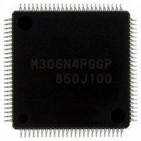
M306N4FGGP#U3 Renesas Electronics America, M306N4FGGP#U3 Datasheet - Page 276

M306N4FGGP#U3
Manufacturer Part Number
M306N4FGGP#U3
Description
IC M16C/6N4 MCU FLASH 100-LQFP
Manufacturer
Renesas Electronics America
Series
M16C™ M16C/6Nr
Specifications of M306N4FGGP#U3
Core Processor
M16C/60
Core Size
16-Bit
Speed
24MHz
Connectivity
CAN, I²C, IEBus, SIO, UART/USART
Peripherals
DMA, WDT
Number Of I /o
85
Program Memory Size
256KB (256K x 8)
Program Memory Type
FLASH
Ram Size
10K x 8
Voltage - Supply (vcc/vdd)
3 V ~ 5.5 V
Data Converters
A/D 26x10b; D/A 2x8b
Oscillator Type
Internal
Operating Temperature
-40°C ~ 85°C
Package / Case
100-LQFP
Package
100LQFP
Family Name
M16C
Maximum Speed
24 MHz
Operating Supply Voltage
3.3|5 V
Data Bus Width
16|32 Bit
Number Of Programmable I/os
87
Interface Type
I2C/UART
On-chip Adc
26-chx10-bit
On-chip Dac
2-chx8-bit
Number Of Timers
11
For Use With
R0K3306NKS001BE - KIT DEV RSK RSK-M16C/6NKR0K3306NKS000BE - KIT DEV RSK RSK-M16C/6NK
Lead Free Status / RoHS Status
Lead free / RoHS Compliant
Eeprom Size
-
Available stocks
Company
Part Number
Manufacturer
Quantity
Price
- Current page: 276 of 414
- Download datasheet (3Mb)
M16C/6N Group (M16C/6N4)
Rev.2.40
REJ09B0009-0240
21.1 Memory Map
Figure 21.1 Flash Memory Block Diagram
The flash memory contains the user ROM area and the boot ROM area. The user ROM area has space to
store the MCU operating program in single-chip mode or memory expansion mode and a separate 4-Kbyte
space as the block A.
Figure 21.1 shows the Flash Memory Block Diagram.
The user ROM area is divided into several blocks, each of which can be protected (locked) against
programming or erasure. The user ROM area can be rewritten in CPU rewrite, standard serial I/O mode,
parallel I/O mode, and CAN I/O mode. Block A is enabled for use by setting the PM10 bit in the PM1 register
to 1 (block A enabled. CS2 area at addresses 10000h to 26FFFh).
The boot ROM area is located at the same addresses as the user ROM area. It can only be rewritten in
parallel I/O mode (refer to 21.1.1 Boot Mode). A program in the boot ROM area is executed after a hardware
reset occurs while an “H ” signal is applied to pins CNVSS and P5_0 and an “L” signal is applied to the P5_5
pin (refer to 21.1.1 Boot Mode). A program in the user ROM area is executed after a hardware reset occurs
while an “L” signal is applied to the CNVSS pin. However, the boot ROM area cannot be read.
21.1.1 Boot Mode
The MCU enters boot mode when a hardware reset occurs while an “H ” signal is applied to pins CNVSS
and P5_0 and an “L ” signal is applied to the P5_5 pin. A program in the boot ROM area is executed.
In boot mode, the FMR05 bit in the FMR0 register selects access to the boot ROM area or the user ROM area.
The rewrite control program for standard serial I/O mode is stored in the boot ROM area before shipment.
The boot ROM area can be rewritten in parallel I/O mode only. If given rewrite control program using
erase-write mode (EW0 mode) is written in the boot ROM area, the flash memory can be rewritten
according to the system implemented.
Apr 14, 2006
* Shown here is a block diagram during single-chip mode.
NOTES:
0DFFFFh
0E0000h
0C0000h
0CFFFFh
0D0000h
0FFFFFh
00F000h
00FFFFh
0EFFFFh
0F0000h
1. Block A can be made usable by setting the PM10 bit in the PM1 register to 1 (block A enabled, addresses
2. The boot ROM area can only be rewritten in parallel I/O mode.
3. To specify a block, use an even address in that block.
10000h to 26FFFh for CS2 area).
Block A cannot be erased by the erase all unlocked block command. Use the block erase command to
erase it.
page 252 of 376
(32+8+8+8+4+4) Kbytes
Block A: 4 Kbytes
Block 8: 64 Kbytes
Block 7: 64 Kbytes
Block 6: 64 Kbytes
_______
Block 5 to 0
(1)
User ROM area
0F0000h
0F7FFFh
0F8000h
0F9FFFh
0FA000h
0FBFFFh
0FC000h
0FDFFFh
0FE000h
0FEFFFh
0FF000h
0FFFFFh
Block 5: 32 Kbytes
Block 4: 8 Kbytes
Block 3: 8 Kbytes
Block 2: 8 Kbytes
Block 1: 4 Kbytes
Block 0: 4 Kbytes
0FF000h
0FFFFFh
Boot ROM area
4 Kbytes
21. Flash Memory Version
(2)
Related parts for M306N4FGGP#U3
Image
Part Number
Description
Manufacturer
Datasheet
Request
R

Part Number:
Description:
KIT STARTER FOR M16C/29
Manufacturer:
Renesas Electronics America
Datasheet:

Part Number:
Description:
KIT STARTER FOR R8C/2D
Manufacturer:
Renesas Electronics America
Datasheet:

Part Number:
Description:
R0K33062P STARTER KIT
Manufacturer:
Renesas Electronics America
Datasheet:

Part Number:
Description:
KIT STARTER FOR R8C/23 E8A
Manufacturer:
Renesas Electronics America
Datasheet:

Part Number:
Description:
KIT STARTER FOR R8C/25
Manufacturer:
Renesas Electronics America
Datasheet:

Part Number:
Description:
KIT STARTER H8S2456 SHARPE DSPLY
Manufacturer:
Renesas Electronics America
Datasheet:

Part Number:
Description:
KIT STARTER FOR R8C38C
Manufacturer:
Renesas Electronics America
Datasheet:

Part Number:
Description:
KIT STARTER FOR R8C35C
Manufacturer:
Renesas Electronics America
Datasheet:

Part Number:
Description:
KIT STARTER FOR R8CL3AC+LCD APPS
Manufacturer:
Renesas Electronics America
Datasheet:

Part Number:
Description:
KIT STARTER FOR RX610
Manufacturer:
Renesas Electronics America
Datasheet:

Part Number:
Description:
KIT STARTER FOR R32C/118
Manufacturer:
Renesas Electronics America
Datasheet:

Part Number:
Description:
KIT DEV RSK-R8C/26-29
Manufacturer:
Renesas Electronics America
Datasheet:

Part Number:
Description:
KIT STARTER FOR SH7124
Manufacturer:
Renesas Electronics America
Datasheet:

Part Number:
Description:
KIT STARTER FOR H8SX/1622
Manufacturer:
Renesas Electronics America
Datasheet:

Part Number:
Description:
KIT DEV FOR SH7203
Manufacturer:
Renesas Electronics America
Datasheet:


