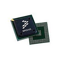
MPC5125YVN400 Freescale Semiconductor, MPC5125YVN400 Datasheet - Page 882

MPC5125YVN400
Manufacturer Part Number
MPC5125YVN400
Description
IC MCU 32BIT E300 324TEPBGA
Manufacturer
Freescale Semiconductor
Series
MPC51xxr
Datasheets
1.MPC5125YVN400.pdf
(92 pages)
2.MPC5125YVN400.pdf
(8 pages)
3.MPC5125YVN400.pdf
(2 pages)
4.MPC5125YVN400.pdf
(1064 pages)
Specifications of MPC5125YVN400
Core Processor
e300
Core Size
32-Bit
Speed
400MHz
Connectivity
CAN, EBI/EMI, Ethernet, I²C, USB OTG
Peripherals
DMA, WDT
Number Of I /o
64
Program Memory Type
ROMless
Ram Size
32K x 8
Voltage - Supply (vcc/vdd)
1.33 V ~ 1.47 V
Oscillator Type
External
Operating Temperature
-40°C ~ 125°C
Package / Case
324-PBGA
Processor Series
MPC51xx
Core
e300
Data Bus Width
32 bit
Development Tools By Supplier
TWR-MPC5125-KIT, TWR-SER, TWR-ELEV, TOWER
Maximum Clock Frequency
400 MHz
Operating Supply Voltage
1.4 V
Maximum Operating Temperature
+ 125 C
Mounting Style
SMD/SMT
Data Ram Size
32 KB
I/o Voltage
3.3 V
Interface Type
CAN, I2C
Minimum Operating Temperature
- 40 C
Program Memory Size
32 bit
Cpu Speed
400MHz
Embedded Interface Type
CAN, I2C, SPI, UART, USB
Digital Ic Case Style
TEPBGA
No. Of Pins
324
Rohs Compliant
Yes
Cpu Family
MPC5xx
Device Core Size
32b
Frequency (max)
400MHz
Total Internal Ram Size
32KB
Instruction Set Architecture
RISC
Operating Temp Range
-40C to 85C
Operating Temperature Classification
Industrial
Mounting
Surface Mount
Pin Count
324
Lead Free Status / RoHS Status
Lead free / RoHS Compliant
Eeprom Size
-
Program Memory Size
-
Data Converters
-
Lead Free Status / Rohs Status
Lead free / RoHS Compliant
Available stocks
Company
Part Number
Manufacturer
Quantity
Price
Company:
Part Number:
MPC5125YVN400
Manufacturer:
Freescale Semiconductor
Quantity:
135
Company:
Part Number:
MPC5125YVN400
Manufacturer:
LTC
Quantity:
29
Company:
Part Number:
MPC5125YVN400
Manufacturer:
Freescale Semiconductor
Quantity:
10 000
- MPC5125YVN400 PDF datasheet
- MPC5125YVN400 PDF datasheet #2
- MPC5125YVN400 PDF datasheet #3
- MPC5125YVN400 PDF datasheet #4
- Current page: 882 of 1064
- Download datasheet (6Mb)
Universal Serial Bus Interface with On-The-Go
32.3
Both modules, USB1/USB2, can be broken down into functional sub-blocks described below.
32.3.1
The system interface block contains all the control and status registers that allow the CPU core to interface
to the module. These registers allow the processor to control the configuration of the module, ascertain the
capabilities of each module and control the module’s operation.
32-54
Address: Base + 0x200
WU_INT_CLR Wake-up Interrupt clear.
WU_ULPI_EN Wakeup on ULPI Interrupt Event. This bit is used to enable the wake up from the ULPI I/F.
ULPI_SEL
Reset
Reset
WU_IE
Field
PPP
PFP
W
W
R
R
Functional Description
16
0
0
0
0
0
System Interface
0 Default, no action.
1 Clear the wake-up interrupt.
ULPI I/F Select Not used in this implementation.
Port Power Polarity. Not used in this implementation.
Power Fault Polarity. Not used in this implementation.
0 Wake Up Interrupt Disabled.
1 Wake Up Interrupt Enabled.
WAKEUP INTERRUPT ENABLE. This bit is used to enable the low power wakeup interrupt.
0 Low power wakeup interrupt disabled.
1 Low power wakeup interrupt enabled.
17
0
0
0
0
1
Figure 32-41. USB General Control (USB_USBGENCTRL) Register
18
0
0
0
0
2
Table 32-42. USB_USBGENCTRL field descriptions
19
0
0
0
0
3
MPC5125 Microcontroller Reference Manual, Rev. 2
20
4
0
0
0
0
21
0
0
0
0
5
22
0
0
0
0
6
23
0
0
0
0
7
Description
24
8
0
0
0
0
25
9
0
0
0
0
_CLR
_INT
w1c
WU
10
26
0
0
0
_SEL
ULPI
11
27
0
0
0
PPP
12
28
0
0
0
Freescale Semiconductor
Access: User read/write
PFP
13
29
0
0
0
_ULPI
_EN
WU
14
30
0
0
0
WU
_IE
15
31
0
0
0
Related parts for MPC5125YVN400
Image
Part Number
Description
Manufacturer
Datasheet
Request
R
Part Number:
Description:
Mpc5125 Microcontroller Data Sheet
Manufacturer:
Freescale Semiconductor, Inc
Datasheet:

Part Number:
Description:
MPC5125 Microcontroller Data Sheet
Manufacturer:
FREESCALE [Freescale Semiconductor, Inc]
Datasheet:
Part Number:
Description:
Manufacturer:
Freescale Semiconductor, Inc
Datasheet:
Part Number:
Description:
Manufacturer:
Freescale Semiconductor, Inc
Datasheet:
Part Number:
Description:
Manufacturer:
Freescale Semiconductor, Inc
Datasheet:
Part Number:
Description:
Manufacturer:
Freescale Semiconductor, Inc
Datasheet:
Part Number:
Description:
Manufacturer:
Freescale Semiconductor, Inc
Datasheet:
Part Number:
Description:
Manufacturer:
Freescale Semiconductor, Inc
Datasheet:
Part Number:
Description:
Manufacturer:
Freescale Semiconductor, Inc
Datasheet:
Part Number:
Description:
Manufacturer:
Freescale Semiconductor, Inc
Datasheet:
Part Number:
Description:
Manufacturer:
Freescale Semiconductor, Inc
Datasheet:
Part Number:
Description:
Manufacturer:
Freescale Semiconductor, Inc
Datasheet:
Part Number:
Description:
Manufacturer:
Freescale Semiconductor, Inc
Datasheet:
Part Number:
Description:
Manufacturer:
Freescale Semiconductor, Inc
Datasheet:
Part Number:
Description:
Manufacturer:
Freescale Semiconductor, Inc
Datasheet:


