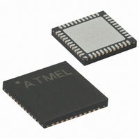
ATMEGA8515-16MU Atmel, ATMEGA8515-16MU Datasheet - Page 66

ATMEGA8515-16MU
Manufacturer Part Number
ATMEGA8515-16MU
Description
IC AVR MCU 8K 16MHZ 5V 44-QFN
Manufacturer
Atmel
Series
AVR® ATmegar
Specifications of ATMEGA8515-16MU
Core Processor
AVR
Core Size
8-Bit
Speed
16MHz
Connectivity
EBI/EMI, SPI, UART/USART
Peripherals
Brown-out Detect/Reset, POR, PWM, WDT
Number Of I /o
35
Program Memory Size
8KB (4K x 16)
Program Memory Type
FLASH
Eeprom Size
512 x 8
Ram Size
512 x 8
Voltage - Supply (vcc/vdd)
4.5 V ~ 5.5 V
Oscillator Type
Internal
Operating Temperature
-40°C ~ 85°C
Package / Case
44-VQFN Exposed Pad
Processor Series
ATMEGA8x
Core
AVR8
Data Bus Width
8 bit
Data Ram Size
512 B
Interface Type
SPI, USART
Maximum Clock Frequency
16 MHz
Number Of Programmable I/os
35
Number Of Timers
2
Operating Supply Voltage
4.5 V to 5.5 V
Maximum Operating Temperature
+ 85 C
Mounting Style
SMD/SMT
3rd Party Development Tools
EWAVR, EWAVR-BL
Development Tools By Supplier
ATAVRDRAGON, ATSTK500, ATSTK600, ATAVRISP2, ATAVRONEKIT
Minimum Operating Temperature
- 40 C
For Use With
ATAVRISP2 - PROGRAMMER AVR IN SYSTEMATSTK500 - PROGRAMMER AVR STARTER KIT
Lead Free Status / RoHS Status
Lead free / RoHS Compliant
Data Converters
-
Lead Free Status / Rohs Status
Details
- Current page: 66 of 257
- Download datasheet (2Mb)
Special Function IO Register –
SFIOR
Alternate Functions of Port A
66
ATmega8515(L)
• Bit 2 – PUD: Pull-up Disable
When this bit is written to one, the pull-ups in the I/O ports are disabled even if the DDxn
and PORTxn Registers are configured to enable the pull-ups ({DDxn, PORTxn} = 0b01).
See “Configuring the Pin” on page 60 for more details about this feature.
Port A has an alternate function as the address low byte and data lines for the External
Memory Interface.
Table 26. Port A Pins Alternate Functions
Table 27 and Table 28 relate the alternate functions of Port A to the overriding signals
shown in Figure 33 on page 64.
Table 27. Overriding Signals for Alternate Functions in PA7..PA4
Note:
Bit
Read/Write
Initial Value
Signal
Name
PUOE
PUOV
DDOE
DDOV
PVOE
PVOV
DIEOE
DIEOV
DI
AIO
Port Pin
PA7
PA6
PA5
PA4
PA3
PA2
PA1
PA0
1. ADA is short for ADdress Active and represents the time when address is output. See
“External Memory Interface” on page 25.
PA7/AD7
SRE
~(WR | ADA
PortA7
SRE
WR | ADA
SRE
A7 • ADA |
D7 OUTPUT • WR
0
0
D7 INPUT
–
R/W
7
–
0
Alternate Function
AD7 (External memory interface address and data bit 7)
AD6 (External memory interface address and data bit 6)
AD5 (External memory interface address and data bit 5)
AD4 (External memory interface address and data bit 4)
AD3 (External memory interface address and data bit 3)
AD2 (External memory interface address and data bit 2)
AD1 (External memory interface address and data bit 1)
AD0 (External memory interface address and data bit 0)
XMBK
R/W
(1)
6
0
) •
XMM2
R/W
PA6/AD6
SRE
~(WR | ADA) •
PortA6
SRE
WR | ADA
SRE
A6 • ADA |
D6 OUTPUT •
WR
0
0
D6 INPUT
–
5
0
XMM1
R/W
4
0
XMM0
R/W
3
0
PA5/AD5
SRE
~(WR | ADA) •
PortA5
SRE
WR | ADA
SRE
A5 • ADA |
D5 OUTPUT •
WR
0
0
D5 INPUT
–
PUD
R/W
2
0
R/W
1
–
0
PA4/AD4
~(WR | ADA) •
PortA4
SRE
WR | ADA
A4 • ADA |
D4 OUTPUT •
WR
0
0
D4 INPUT
–
SRE
SRE
PSR10
R/W
2512K–AVR–01/10
0
0
SFIOR
Related parts for ATMEGA8515-16MU
Image
Part Number
Description
Manufacturer
Datasheet
Request
R

Part Number:
Description:
IC AVR MCU 2.4GHZ XCEIVER 64QFN
Manufacturer:
Atmel
Datasheet:

Part Number:
Description:
Manufacturer:
Atmel
Datasheet:

Part Number:
Description:
MCU ATMEGA644/AT86RF230 40-DIP
Manufacturer:
Atmel
Datasheet:

Part Number:
Description:
BUNDLE ATMEGA644P/AT86RF230 QFN
Manufacturer:
Atmel
Datasheet:

Part Number:
Description:
BUNDLE ATMEGA644P/AT86RF230 TQFP
Manufacturer:
Atmel
Datasheet:

Part Number:
Description:
MCU ATMEGA1281/AT86RF230 64-TQFP
Manufacturer:
Atmel
Datasheet:

Part Number:
Description:
MCU ATMEGA1280/AT86RF230 100TQFP
Manufacturer:
Atmel
Datasheet:

Part Number:
Description:
BUNDLE ATMEGA1280/AT86RF100-TQFP
Manufacturer:
Atmel
Datasheet:

Part Number:
Description:
BUNDLE ATMEGA2560V/AT86RF230-ZU
Manufacturer:
Atmel
Datasheet:

Part Number:
Description:
MCU ATMEGA2561/AT86RF230 64-TQFP
Manufacturer:
Atmel
Datasheet:

Part Number:
Description:
INTERVAL AND WIPE/WASH WIPER CONTROL IC WITH DELAY
Manufacturer:
ATMEL Corporation
Datasheet:

Part Number:
Description:
Low-Voltage Voice-Switched IC for Hands-Free Operation
Manufacturer:
ATMEL Corporation
Datasheet:

Part Number:
Description:
MONOLITHIC INTEGRATED FEATUREPHONE CIRCUIT
Manufacturer:
ATMEL Corporation
Datasheet:

Part Number:
Description:
AM-FM Receiver IC U4255BM-M
Manufacturer:
ATMEL Corporation
Datasheet:


