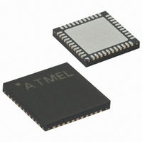
ATMEGA8515-16MU Atmel, ATMEGA8515-16MU Datasheet - Page 95

ATMEGA8515-16MU
Manufacturer Part Number
ATMEGA8515-16MU
Description
IC AVR MCU 8K 16MHZ 5V 44-QFN
Manufacturer
Atmel
Series
AVR® ATmegar
Specifications of ATMEGA8515-16MU
Core Processor
AVR
Core Size
8-Bit
Speed
16MHz
Connectivity
EBI/EMI, SPI, UART/USART
Peripherals
Brown-out Detect/Reset, POR, PWM, WDT
Number Of I /o
35
Program Memory Size
8KB (4K x 16)
Program Memory Type
FLASH
Eeprom Size
512 x 8
Ram Size
512 x 8
Voltage - Supply (vcc/vdd)
4.5 V ~ 5.5 V
Oscillator Type
Internal
Operating Temperature
-40°C ~ 85°C
Package / Case
44-VQFN Exposed Pad
Processor Series
ATMEGA8x
Core
AVR8
Data Bus Width
8 bit
Data Ram Size
512 B
Interface Type
SPI, USART
Maximum Clock Frequency
16 MHz
Number Of Programmable I/os
35
Number Of Timers
2
Operating Supply Voltage
4.5 V to 5.5 V
Maximum Operating Temperature
+ 85 C
Mounting Style
SMD/SMT
3rd Party Development Tools
EWAVR, EWAVR-BL
Development Tools By Supplier
ATAVRDRAGON, ATSTK500, ATSTK600, ATAVRISP2, ATAVRONEKIT
Minimum Operating Temperature
- 40 C
For Use With
ATAVRISP2 - PROGRAMMER AVR IN SYSTEMATSTK500 - PROGRAMMER AVR STARTER KIT
Lead Free Status / RoHS Status
Lead free / RoHS Compliant
Data Converters
-
Lead Free Status / Rohs Status
Details
- Current page: 95 of 257
- Download datasheet (2Mb)
Timer/Counter0 and
Timer/Counter1
Prescalers
Internal Clock Source
Prescaler Reset
External Clock Source
2512K–AVR–01/10
Timer/Counter1 and Timer/Counter0 share the same prescaler module, but the
Timer/Counters can have different prescaler settings. The description below applies to
both Timer/Counter1 and Timer/Counter0.
The Timer/Counter can be clocked directly by the system clock (by setting the
CSn2:0 = 1). This provides the fastest operation, with a maximum Timer/Counter clock
frequency equal to system clock frequency (f
the prescaler can be used as a clock source. The prescaled clock has a frequency of
either f
The prescaler is free running, i.e., operates independently of the clock select logic of the
Timer/Counter, and it is shared by Timer/Counter1 and Timer/Counter0. Since the pres-
caler is not affected by the Timer/Counter’s clock select, the state of the prescaler will
have implications for situations where a prescaled clock is used. One example of pres-
caling artifacts occurs when the timer is enabled and clocked by the prescaler
(6 > CSn2:0 > 1). The number of system clock cycles from when the timer is enabled to
the first count occurs can be from 1 to N+1 system clock cycles, where N equals the
prescaler divisor (8, 64, 256, or 1024).
It is possible to use the Prescaler Reset for synchronizing the Timer/Counter to program
execution. However, care must be taken if the other Timer/Counter that shares the
same prescaler also uses prescaling. A Prescaler Reset will affect the prescaler period
for all Timer/Counters it is connected to.
An external clock source applied to the T1/T0 pin can be used as Timer/Counter clock
(clk
chronization logic. The synchronized (sampled) signal is then passed through the edge
detector. Figure 45 shows a functional equivalent block diagram of the T1/T0 synchroni-
zation and edge detector logic. The registers are clocked at the positive edge of the
internal system clock (
system clock.
The edge detector generates one clk
ative (CSn2:0 = 6) edge it detects.
Figure 45. T1/T0 Pin Sampling
The synchronization and edge detector logic introduces a delay of 2.5 to 3.5 system
clock cycles from an edge has been applied to the T1/T0 pin to the counter is updated.
Enabling and disabling of the clock input must be done when T1/T0 has been stable for
at least one system clock cycle, otherwise it is a risk that a false Timer/Counter clock
pulse is generated.
Each half period of the external clock applied must be longer than one system clock
cycle to ensure correct sampling. The external clock must be guaranteed to have less
than half the system clock frequency (f
Tn
T1
clk
/clk
I/O
CLK_I/O
T0
). The T1/T0 pin is sampled once every system clock cycle by the pin syn-
/8, f
D
LE
CLK_I/O
Q
Synchronization
/64, f
clk
D
I/O
). The latch is transparent in the high period of the internal
CLK_I/O
Q
/256, or f
T1
/clk
ExtClk
T
0
CLK_I/O
< f
pulse for each positive (CSn2:0 = 7) or neg-
CLK_I/O
clk_I/O
/1024.
). Alternatively, one of four taps from
/2) given a 50/50% duty cycle. Since
D
ATmega8515(L)
Q
Edge Detector
Tn_sync
(To Clock
Select Logic)
95
Related parts for ATMEGA8515-16MU
Image
Part Number
Description
Manufacturer
Datasheet
Request
R

Part Number:
Description:
IC AVR MCU 2.4GHZ XCEIVER 64QFN
Manufacturer:
Atmel
Datasheet:

Part Number:
Description:
Manufacturer:
Atmel
Datasheet:

Part Number:
Description:
MCU ATMEGA644/AT86RF230 40-DIP
Manufacturer:
Atmel
Datasheet:

Part Number:
Description:
BUNDLE ATMEGA644P/AT86RF230 QFN
Manufacturer:
Atmel
Datasheet:

Part Number:
Description:
BUNDLE ATMEGA644P/AT86RF230 TQFP
Manufacturer:
Atmel
Datasheet:

Part Number:
Description:
MCU ATMEGA1281/AT86RF230 64-TQFP
Manufacturer:
Atmel
Datasheet:

Part Number:
Description:
MCU ATMEGA1280/AT86RF230 100TQFP
Manufacturer:
Atmel
Datasheet:

Part Number:
Description:
BUNDLE ATMEGA1280/AT86RF100-TQFP
Manufacturer:
Atmel
Datasheet:

Part Number:
Description:
BUNDLE ATMEGA2560V/AT86RF230-ZU
Manufacturer:
Atmel
Datasheet:

Part Number:
Description:
MCU ATMEGA2561/AT86RF230 64-TQFP
Manufacturer:
Atmel
Datasheet:

Part Number:
Description:
INTERVAL AND WIPE/WASH WIPER CONTROL IC WITH DELAY
Manufacturer:
ATMEL Corporation
Datasheet:

Part Number:
Description:
Low-Voltage Voice-Switched IC for Hands-Free Operation
Manufacturer:
ATMEL Corporation
Datasheet:

Part Number:
Description:
MONOLITHIC INTEGRATED FEATUREPHONE CIRCUIT
Manufacturer:
ATMEL Corporation
Datasheet:

Part Number:
Description:
AM-FM Receiver IC U4255BM-M
Manufacturer:
ATMEL Corporation
Datasheet:


