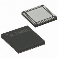
ATMEGA8515-16MU Atmel, ATMEGA8515-16MU Datasheet - Page 87

ATMEGA8515-16MU
Manufacturer Part Number
ATMEGA8515-16MU
Description
IC AVR MCU 8K 16MHZ 5V 44-QFN
Manufacturer
Atmel
Series
AVR® ATmegar
Specifications of ATMEGA8515-16MU
Core Processor
AVR
Core Size
8-Bit
Speed
16MHz
Connectivity
EBI/EMI, SPI, UART/USART
Peripherals
Brown-out Detect/Reset, POR, PWM, WDT
Number Of I /o
35
Program Memory Size
8KB (4K x 16)
Program Memory Type
FLASH
Eeprom Size
512 x 8
Ram Size
512 x 8
Voltage - Supply (vcc/vdd)
4.5 V ~ 5.5 V
Oscillator Type
Internal
Operating Temperature
-40°C ~ 85°C
Package / Case
44-VQFN Exposed Pad
Processor Series
ATMEGA8x
Core
AVR8
Data Bus Width
8 bit
Data Ram Size
512 B
Interface Type
SPI, USART
Maximum Clock Frequency
16 MHz
Number Of Programmable I/os
35
Number Of Timers
2
Operating Supply Voltage
4.5 V to 5.5 V
Maximum Operating Temperature
+ 85 C
Mounting Style
SMD/SMT
3rd Party Development Tools
EWAVR, EWAVR-BL
Development Tools By Supplier
ATAVRDRAGON, ATSTK500, ATSTK600, ATAVRISP2, ATAVRONEKIT
Minimum Operating Temperature
- 40 C
For Use With
ATAVRISP2 - PROGRAMMER AVR IN SYSTEMATSTK500 - PROGRAMMER AVR STARTER KIT
Lead Free Status / RoHS Status
Lead free / RoHS Compliant
Data Converters
-
Lead Free Status / Rohs Status
Details
- Current page: 87 of 257
- Download datasheet (2Mb)
2512K–AVR–01/10
Figure 39. Fast PWM Mode, Timing Diagram
The Timer/Counter Overflow Flag (TOV0) is set each time the counter reaches MAX. If
the interrupt is enabled, the interrupt handler routine can be used for updating the com-
pare value.
In fast PWM mode, the compare unit allows generation of PWM waveforms on the OC0
pin. Setting the COM01:0 bits to 2 will produce a non-inverted PWM and an inverted
PWM output can be generated by setting the COM01:0 to 3 (See Table 46 on page 92).
The actual OC0 value will only be visible on the port pin if the data direction for the port
pin is set as output. The PWM waveform is generated by setting (or clearing) the OC0
Register at the Compare Match between OCR0 and TCNT0, and clearing (or setting)
the OC0 Register at the timer clock cycle the counter is cleared (changes from MAX to
BOTTOM).
The PWM frequency for the output can be calculated by the following equation:
The “N” variable represents the prescale factor (1, 8, 64, 256, or 1024).
The extreme values for the OCR0 Register represents special cases when generating a
PWM waveform output in the fast PWM mode. If the OCR0 is set equal to BOTTOM, the
output will be a narrow spike for each MAX+1 timer clock cycle. Setting the OCR0 equal
to MAX will result in a constantly high or low output (depending on the polarity of the out-
put set by the COM01:0 bits).
A frequency (with 50% duty cycle) waveform output in fast PWM mode can be achieved
by setting OC0 to toggle its logical level on each Compare Match (COM01:0 = 1). The
waveform generated will have a maximum frequency of f
set to zero. This feature is similar to the OC0 toggle in CTC mode, except the double
buffer feature of the output compare unit is enabled in the fast PWM mode.
TCNTn
OCn
OCn
Period
1
2
3
f
OCnPWM
4
=
----------------- -
N 256
f
clk_I/O
⋅
5
ATmega8515(L)
6
OC0
= f
OCRn Interrupt Flag Set
OCRn Update and
TOVn Interrupt Flag Set
clk_I/O
7
(COMn1:0 = 2)
(COMn1:0 = 3)
/2 when OCR0 is
87
Related parts for ATMEGA8515-16MU
Image
Part Number
Description
Manufacturer
Datasheet
Request
R

Part Number:
Description:
IC AVR MCU 2.4GHZ XCEIVER 64QFN
Manufacturer:
Atmel
Datasheet:

Part Number:
Description:
Manufacturer:
Atmel
Datasheet:

Part Number:
Description:
MCU ATMEGA644/AT86RF230 40-DIP
Manufacturer:
Atmel
Datasheet:

Part Number:
Description:
BUNDLE ATMEGA644P/AT86RF230 QFN
Manufacturer:
Atmel
Datasheet:

Part Number:
Description:
BUNDLE ATMEGA644P/AT86RF230 TQFP
Manufacturer:
Atmel
Datasheet:

Part Number:
Description:
MCU ATMEGA1281/AT86RF230 64-TQFP
Manufacturer:
Atmel
Datasheet:

Part Number:
Description:
MCU ATMEGA1280/AT86RF230 100TQFP
Manufacturer:
Atmel
Datasheet:

Part Number:
Description:
BUNDLE ATMEGA1280/AT86RF100-TQFP
Manufacturer:
Atmel
Datasheet:

Part Number:
Description:
BUNDLE ATMEGA2560V/AT86RF230-ZU
Manufacturer:
Atmel
Datasheet:

Part Number:
Description:
MCU ATMEGA2561/AT86RF230 64-TQFP
Manufacturer:
Atmel
Datasheet:

Part Number:
Description:
INTERVAL AND WIPE/WASH WIPER CONTROL IC WITH DELAY
Manufacturer:
ATMEL Corporation
Datasheet:

Part Number:
Description:
Low-Voltage Voice-Switched IC for Hands-Free Operation
Manufacturer:
ATMEL Corporation
Datasheet:

Part Number:
Description:
MONOLITHIC INTEGRATED FEATUREPHONE CIRCUIT
Manufacturer:
ATMEL Corporation
Datasheet:

Part Number:
Description:
AM-FM Receiver IC U4255BM-M
Manufacturer:
ATMEL Corporation
Datasheet:


