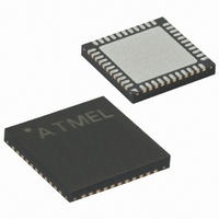
ATMEGA8515-16MU Atmel, ATMEGA8515-16MU Datasheet - Page 93

ATMEGA8515-16MU
Manufacturer Part Number
ATMEGA8515-16MU
Description
IC AVR MCU 8K 16MHZ 5V 44-QFN
Manufacturer
Atmel
Series
AVR® ATmegar
Specifications of ATMEGA8515-16MU
Core Processor
AVR
Core Size
8-Bit
Speed
16MHz
Connectivity
EBI/EMI, SPI, UART/USART
Peripherals
Brown-out Detect/Reset, POR, PWM, WDT
Number Of I /o
35
Program Memory Size
8KB (4K x 16)
Program Memory Type
FLASH
Eeprom Size
512 x 8
Ram Size
512 x 8
Voltage - Supply (vcc/vdd)
4.5 V ~ 5.5 V
Oscillator Type
Internal
Operating Temperature
-40°C ~ 85°C
Package / Case
44-VQFN Exposed Pad
Processor Series
ATMEGA8x
Core
AVR8
Data Bus Width
8 bit
Data Ram Size
512 B
Interface Type
SPI, USART
Maximum Clock Frequency
16 MHz
Number Of Programmable I/os
35
Number Of Timers
2
Operating Supply Voltage
4.5 V to 5.5 V
Maximum Operating Temperature
+ 85 C
Mounting Style
SMD/SMT
3rd Party Development Tools
EWAVR, EWAVR-BL
Development Tools By Supplier
ATAVRDRAGON, ATSTK500, ATSTK600, ATAVRISP2, ATAVRONEKIT
Minimum Operating Temperature
- 40 C
For Use With
ATAVRISP2 - PROGRAMMER AVR IN SYSTEMATSTK500 - PROGRAMMER AVR STARTER KIT
Lead Free Status / RoHS Status
Lead free / RoHS Compliant
Data Converters
-
Lead Free Status / Rohs Status
Details
- Current page: 93 of 257
- Download datasheet (2Mb)
Timer/Counter Register –
TCNT0
Output Compare Register –
OCR0
Timer/Counter Interrupt Mask
Register – TIMSK
2512K–AVR–01/10
The three Clock Select bits select the clock source to be used by the Timer/Counter.
Table 48. Clock Select Bit Description
If external pin modes are used for the Timer/Counter0, transitions on the T0 pin will
clock the counter even if the pin is configured as an output. This feature allows software
control of the counting.
The Timer/Counter Register gives direct access, both for read and write operations, to
the Timer/Counter unit 8-bit counter. Writing to the TCNT0 Register blocks (removes)
the Compare Match on the following timer clock. Modifying the counter (TCNT0) while
the counter is running, introduces a risk of missing a Compare Match between TCNT0
and the OCR0 Register.
The Output Compare Register contains an 8-bit value that is continuously compared
with the counter value (TCNT0). A match can be used to generate an output compare
interrupt, or to generate a waveform output on the OC0 pin.
• Bit 1 – TOIE0: Timer/Counter0 Overflow Interrupt Enable
When the TOIE0 bit is written to one, and the I-bit in the Status Register is set (one), the
Timer/Counter0 Overflow interrupt is enabled. The corresponding interrupt is executed if
an overflow in Timer/Counter0 occurs, i.e., when the TOV0 bit is set in the Timer/Coun-
ter Interrupt Flag Register – TIFR.
• Bit 0 – OCIE0: Timer/Counter0 Output Compare Match Interrupt Enable
Bit
Read/Write
Initial Value
Bit
Read/Write
Initial Value
Bit
Read/Write
Initial Value
CS02
0
0
0
0
1
1
1
1
CS01
0
0
1
1
0
0
1
1
TOIE1
R/W
R/W
R/W
7
0
7
0
7
0
CS00
OCIE1A
0
1
0
1
0
1
0
1
R/W
R/W
R/W
6
0
6
0
6
0
Description
No clock source (Timer/counter stopped).
clk
clk
clk
clk
clk
External clock source on T0 pin. Clock on falling edge.
External clock source on T0 pin. Clock on rising edge.
OCIE1B
R/W
R/W
R/W
I/O
I/O
I/O
I/O
I/O
5
0
5
0
5
0
/(No prescaling)
/8 (From prescaler)
/64 (From prescaler)
/256 (From prescaler)
/1024 (From prescaler)
R/W
R/W
R/W
4
0
4
0
4
–
0
TCNT0[7:0]
OCR0[7:0]
TICIE1
R/W
R/W
R/W
3
0
3
0
3
0
R/W
R/W
R/W
2
0
2
0
ATmega8515(L)
2
–
0
TOIE0
R/W
R/W
R/W
1
0
1
0
1
0
OCIE0
R/W
R/W
R/W
0
0
0
0
0
0
TCNT0
OCR0
TIMSK
93
Related parts for ATMEGA8515-16MU
Image
Part Number
Description
Manufacturer
Datasheet
Request
R

Part Number:
Description:
IC AVR MCU 2.4GHZ XCEIVER 64QFN
Manufacturer:
Atmel
Datasheet:

Part Number:
Description:
Manufacturer:
Atmel
Datasheet:

Part Number:
Description:
MCU ATMEGA644/AT86RF230 40-DIP
Manufacturer:
Atmel
Datasheet:

Part Number:
Description:
BUNDLE ATMEGA644P/AT86RF230 QFN
Manufacturer:
Atmel
Datasheet:

Part Number:
Description:
BUNDLE ATMEGA644P/AT86RF230 TQFP
Manufacturer:
Atmel
Datasheet:

Part Number:
Description:
MCU ATMEGA1281/AT86RF230 64-TQFP
Manufacturer:
Atmel
Datasheet:

Part Number:
Description:
MCU ATMEGA1280/AT86RF230 100TQFP
Manufacturer:
Atmel
Datasheet:

Part Number:
Description:
BUNDLE ATMEGA1280/AT86RF100-TQFP
Manufacturer:
Atmel
Datasheet:

Part Number:
Description:
BUNDLE ATMEGA2560V/AT86RF230-ZU
Manufacturer:
Atmel
Datasheet:

Part Number:
Description:
MCU ATMEGA2561/AT86RF230 64-TQFP
Manufacturer:
Atmel
Datasheet:

Part Number:
Description:
INTERVAL AND WIPE/WASH WIPER CONTROL IC WITH DELAY
Manufacturer:
ATMEL Corporation
Datasheet:

Part Number:
Description:
Low-Voltage Voice-Switched IC for Hands-Free Operation
Manufacturer:
ATMEL Corporation
Datasheet:

Part Number:
Description:
MONOLITHIC INTEGRATED FEATUREPHONE CIRCUIT
Manufacturer:
ATMEL Corporation
Datasheet:

Part Number:
Description:
AM-FM Receiver IC U4255BM-M
Manufacturer:
ATMEL Corporation
Datasheet:


