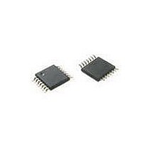
P89LPC9151FDH,129 NXP Semiconductors, P89LPC9151FDH,129 Datasheet - Page 12

P89LPC9151FDH,129
Manufacturer Part Number
P89LPC9151FDH,129
Description
IC 80C51 MCU FLASH 2KB 14TSSOP
Manufacturer
NXP Semiconductors
Series
LPC900r
Datasheet
1.P89LPC9151FDH129.pdf
(91 pages)
Specifications of P89LPC9151FDH,129
Program Memory Type
FLASH
Program Memory Size
2KB (2K x 8)
Package / Case
14-TSSOP
Core Processor
8051
Core Size
8-Bit
Speed
18MHz
Connectivity
I²C, UART/USART
Peripherals
Brown-out Detect/Reset, POR, PWM, WDT
Number Of I /o
12
Ram Size
256 x 8
Voltage - Supply (vcc/vdd)
2.4 V ~ 3.6 V
Data Converters
A/D 4x8b; D/A 1x8b
Oscillator Type
Internal
Operating Temperature
-40°C ~ 85°C
Processor Series
P89LPC
Core
80C51
Data Bus Width
8 bit
Data Ram Size
256 B
Interface Type
SPI
Maximum Clock Frequency
18 MHz
Number Of Programmable I/os
10
Number Of Timers
2
Operating Supply Voltage
2.4 V to 3.6 V
Maximum Operating Temperature
+ 85 C
Mounting Style
SMD/SMT
3rd Party Development Tools
PK51, CA51, A51, ULINK2
Minimum Operating Temperature
- 40 C
On-chip Adc
8 bit, 4 Channel
Lead Free Status / RoHS Status
Lead free / RoHS Compliant
Eeprom Size
-
Lead Free Status / Rohs Status
Lead free / RoHS Compliant
Other names
935290259129
NXP Semiconductors
Table 4.
P89LPC9151_61_71_2
Product data sheet
Symbol
P0.1 to P0.5
P0.1/CIN2B/
KBI1/AD10
P0.2/CIN2A/
KBI2/AD11
P0.3/CIN1B/
KBI3/AD12
P0.4/CIN1A/
KBI4/DAC1/AD13
P0.5/CMPREF/
KBI5
P1.0 to P1.3, P1.5
P1.0/TXD
P1.1/RXD
P89LPC9161 Pin description
Pin
TSSOP16
1
16
15
14
13
10
9
Type Description
I/O
I/O
I
I
I
I/O
I
I
I
I/O
I
I
I
I/O
I
I
O
I
I/O
I
I
I
I/O, I
[1]
I/O
O
I/O
I
Port 0: Port 0 is an 5-bit I/O port with a user-configurable output type. During
reset Port 0 latches are configured in the input only mode with the internal pull-up
disabled. The operation of Port 0 pins as inputs and outputs depends upon the
port configuration selected. Each port pin is configured independently. Refer to
Section 7.15.1 “Port configurations”
details.
The Keypad Interrupt feature operates with Port 0 pins.
All pins have Schmitt trigger inputs.
Port 0 also provides various special functions as described below:
P0.1 — Port 0 bit 1.
CIN2B — Comparator 2 positive input B.
KBI1 — Keyboard input 1.
AD10 — ADC1 channel 0 analog input.
P0.2 — Port 0 bit 2.
CIN2A — Comparator 2 positive input A.
KBI2 — Keyboard input 2.
AD11 — ADC1 channel 1 analog input.
P0.3 — Port 0 bit 3. High current source.
CIN1B — Comparator 1 positive input B.
KBI3 — Keyboard input 3.
AD12 — ADC1 channel 2 analog input.
P0.4 — Port 0 bit 4. High current source.
CIN1A — Comparator 1 positive input A.
KBI4 — Keyboard input 4.
DAC1 — Digital-to-analog converter output 1.
AD13 — ADC1 channel 3 analog input.
P0.5 — Port 0 bit 5. High current source.
CMPREF — Comparator reference (negative) input.
KBI5 — Keyboard input 5.
CLKIN — External clock input.
Port 1: Port 1 is an 5-bit I/O port with a user-configurable output type, except for
three pins as noted below. During reset Port 1 latches are configured in the input
only mode with the internal pull-up disabled. The operation of the configurable
Port 1 pins as inputs and outputs depends upon the port configuration selected.
Each of the configurable port pins are programmed independently. Refer to
Section 7.15.1 “Port configurations”
details. P1.2 to P1.3 are open drain when used as outputs. P1.5 is input only.
All pins have Schmitt trigger inputs.
Port 1 also provides various special functions as described below:
P1.0 — Port 1 bit 0.
TXD — Transmitter output for serial port.
P1.1 — Port 1 bit 1.
RXD — Receiver input for serial port.
Rev. 02 — 9 February 2010
P89LPC9151/9161/9171
and
and
8-bit microcontroller with 8-bit ADC
Table 16 “Static characteristics”
Table 16 “Static characteristics”
© NXP B.V. 2010. All rights reserved.
for
for
12 of 91


