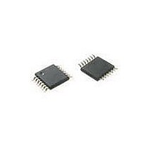
P89LPC9151FDH,129 NXP Semiconductors, P89LPC9151FDH,129 Datasheet - Page 62

P89LPC9151FDH,129
Manufacturer Part Number
P89LPC9151FDH,129
Description
IC 80C51 MCU FLASH 2KB 14TSSOP
Manufacturer
NXP Semiconductors
Series
LPC900r
Datasheet
1.P89LPC9151FDH129.pdf
(91 pages)
Specifications of P89LPC9151FDH,129
Program Memory Type
FLASH
Program Memory Size
2KB (2K x 8)
Package / Case
14-TSSOP
Core Processor
8051
Core Size
8-Bit
Speed
18MHz
Connectivity
I²C, UART/USART
Peripherals
Brown-out Detect/Reset, POR, PWM, WDT
Number Of I /o
12
Ram Size
256 x 8
Voltage - Supply (vcc/vdd)
2.4 V ~ 3.6 V
Data Converters
A/D 4x8b; D/A 1x8b
Oscillator Type
Internal
Operating Temperature
-40°C ~ 85°C
Processor Series
P89LPC
Core
80C51
Data Bus Width
8 bit
Data Ram Size
256 B
Interface Type
SPI
Maximum Clock Frequency
18 MHz
Number Of Programmable I/os
10
Number Of Timers
2
Operating Supply Voltage
2.4 V to 3.6 V
Maximum Operating Temperature
+ 85 C
Mounting Style
SMD/SMT
3rd Party Development Tools
PK51, CA51, A51, ULINK2
Minimum Operating Temperature
- 40 C
On-chip Adc
8 bit, 4 Channel
Lead Free Status / RoHS Status
Lead free / RoHS Compliant
Eeprom Size
-
Lead Free Status / Rohs Status
Lead free / RoHS Compliant
Other names
935290259129
NXP Semiconductors
P89LPC9151_61_71_2
Product data sheet
8.4.5 Dual channel, continuous conversion mode
8.4.6 Single step mode
8.5.1 Timer triggered start
8.5.2 Start immediately
8.5.3 Edge triggered
8.5 Conversion start modes
8.6 Boundary limits interrupt
all selected channels have been converted. The process will repeat starting with the first
selected channel. Additional conversion results will again cycle through the four result
register pairs, overwriting the previous results. Continuous conversions continue until
terminated by the user.
This is a variation of the auto scan continuous conversion mode where conversion occurs
on two user-selectable inputs. The result of the conversion of the first channel is placed in
the result register, AD1DAT0. The result of the conversion of the second channel is placed
in result register, AD1DAT1. The first channel is again converted and its result stored in
AD1DAT2. The second channel is again converted and its result placed in AD1DAT3. An
interrupt is generated, if enabled, after every set of four conversions (two conversions per
channel).
This special mode allows ‘single-stepping’ in an auto scan conversion mode. Any
combination of the four input channels can be selected for conversion. After each channel
is converted, an interrupt is generated, if enabled, and the A/D waits for the next start
condition. May be used with any of the start modes.
An A/D conversion is started by the overflow of Timer 0. Once a conversion has started,
additional Timer 0 triggers are ignored until the conversion has completed. The Timer
triggered start mode is available in all ADC operating modes.
Programming this mode immediately starts a conversion. This start mode is available in all
ADC operating modes.
An A/D conversion is started by rising or falling edge of P1.4. Once a conversion has
started, additional edge triggers are ignored until the conversion has completed. The edge
triggered start mode is available in all ADC operating modes.
Each of the A/D converters has both a high and low boundary limit register. The user may
select whether an interrupt is generated when the conversion result is within (or equal to)
the high and low boundary limits or when the conversion result is outside the boundary
limits. An interrupt will be generated, if enabled, if the result meets the selected interrupt
criteria. The boundary limit may be disabled by clearing the boundary limit interrupt
enable.
An early detection mechanism exists when the interrupt criteria has been selected to be
outside the boundary limits. In this case, after the four MSBs have been converted, these
four bits are compared with the four MSBs of the boundary high and low registers. If the
four MSBs of the conversion meet the interrupt criteria (i.e., outside the boundary limits)
an interrupt will be generated, if enabled. If the four MSBs do not meet the interrupt
Rev. 02 — 9 February 2010
P89LPC9151/9161/9171
8-bit microcontroller with 8-bit ADC
© NXP B.V. 2010. All rights reserved.
62 of 91


