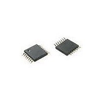
P89LPC9151FDH,129 NXP Semiconductors, P89LPC9151FDH,129 Datasheet - Page 39

P89LPC9151FDH,129
Manufacturer Part Number
P89LPC9151FDH,129
Description
IC 80C51 MCU FLASH 2KB 14TSSOP
Manufacturer
NXP Semiconductors
Series
LPC900r
Datasheet
1.P89LPC9151FDH129.pdf
(91 pages)
Specifications of P89LPC9151FDH,129
Program Memory Type
FLASH
Program Memory Size
2KB (2K x 8)
Package / Case
14-TSSOP
Core Processor
8051
Core Size
8-Bit
Speed
18MHz
Connectivity
I²C, UART/USART
Peripherals
Brown-out Detect/Reset, POR, PWM, WDT
Number Of I /o
12
Ram Size
256 x 8
Voltage - Supply (vcc/vdd)
2.4 V ~ 3.6 V
Data Converters
A/D 4x8b; D/A 1x8b
Oscillator Type
Internal
Operating Temperature
-40°C ~ 85°C
Processor Series
P89LPC
Core
80C51
Data Bus Width
8 bit
Data Ram Size
256 B
Interface Type
SPI
Maximum Clock Frequency
18 MHz
Number Of Programmable I/os
10
Number Of Timers
2
Operating Supply Voltage
2.4 V to 3.6 V
Maximum Operating Temperature
+ 85 C
Mounting Style
SMD/SMT
3rd Party Development Tools
PK51, CA51, A51, ULINK2
Minimum Operating Temperature
- 40 C
On-chip Adc
8 bit, 4 Channel
Lead Free Status / RoHS Status
Lead free / RoHS Compliant
Eeprom Size
-
Lead Free Status / Rohs Status
Lead free / RoHS Compliant
Other names
935290259129
NXP Semiconductors
P89LPC9151_61_71_2
Product data sheet
Fig 10. Block diagram of oscillator control
(7.3728 MHz/14.7456 MHz ± 1 %)
7.6 Watchdog oscillator option
7.7 External clock input option
7.8 Clock sources switch on the fly
(400 kHz ± 5 %)
OSCILLATOR
OSCILLATOR
CLKIN
WATCHDOG
running at 8 MHz or slower. When clock doubler option is enabled, BOE1 bit (UCFG1.5)
and BOE0 bit (UCFG1.3) are required to hold the device in reset at power-up until V
has reached its specified level.
The watchdog has a separate oscillator which has a frequency of 400 kHz, calibrated to
±5 % at room temperature. This oscillator can be used to save power when a high clock
frequency is not needed.
In this configuration, the processor clock is derived from an external source driving the
P0.5/CLKIN pin. The rate may be from 0 Hz up to 18 MHz. When the frequency above
12 MHz, BOE1 bit (UCFG1.5) and BOE0 bit (UCFG1.3) are required to hold the device in
reset at power-up until V
Remark: When using P0.5 as a clock input option, please make sure that P0.5 is
configured as input only mode.
P89LPC9151/9161/9171 can implement clock source switch in any sources of watchdog
oscillator, 7 MHz/14 MHz IRC oscillator, or external clock input during code is running.
CLKOK bit in CLKCON register is used to indicate the clock switch status. CLKOK is
cleared when starting clock source switch and set when completed. Notice that when
CLKOK is ‘0’, writing to CLKCON register is not allowed.
RC
RCCLK
Rev. 02 — 9 February 2010
RCCLK
DD
has reached its specified level.
XCLK
DIVM
TIMER 0 AND
TIMER 1
OSCCLK
P89LPC9151/9161/9171
PCLK
I
2
C-BUS
÷2
RTCS1:0
CCLK
PCLK
8-bit microcontroller with 8-bit ADC
UART
ADC1/DAC1
WDT
CPU
RTC
CLKOUT
(P89LPC9161)
002aae574
SPI
© NXP B.V. 2010. All rights reserved.
39 of 91
DD


