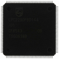
LPC2290FBD144/01,5 NXP Semiconductors, LPC2290FBD144/01,5 Datasheet - Page 20

LPC2290FBD144/01,5
Manufacturer Part Number
LPC2290FBD144/01,5
Description
IC ARM7 MCU RAM 16K 144-LQFP
Manufacturer
NXP Semiconductors
Series
LPC2200r
Datasheet
1.LPC2290FBD144015.pdf
(41 pages)
Specifications of LPC2290FBD144/01,5
Package / Case
144-LQFP
Core Processor
ARM7
Core Size
16/32-Bit
Speed
60MHz
Connectivity
CAN, EBI/EMI, I²C, Microwire, SPI, SSI, SSP, UART/USART
Peripherals
PWM, WDT
Number Of I /o
76
Program Memory Type
ROMless
Ram Size
64K x 8
Voltage - Supply (vcc/vdd)
1.65 V ~ 3.6 V
Data Converters
A/D 8x10b
Oscillator Type
Internal
Operating Temperature
-40°C ~ 85°C
Processor Series
LPC22
Core
ARM7TDMI-S
Data Bus Width
16 bit, 32 bit
Data Ram Size
64 KB
Interface Type
CAN/I2C/SPI/UART
Maximum Clock Frequency
72 MHz
Number Of Programmable I/os
76
Number Of Timers
2
Operating Supply Voltage
3.3 V
Maximum Operating Temperature
+ 85 C
Mounting Style
SMD/SMT
3rd Party Development Tools
MDK-ARM, RL-ARM, ULINK2
Minimum Operating Temperature
- 40 C
On-chip Adc
8-ch x 10-bit
Package
144LQFP
Device Core
ARM7TDMI-S
Family Name
LPC2000
Maximum Speed
72 MHz
Lead Free Status / RoHS Status
Lead free / RoHS Compliant
For Use With
OM10091 - KIT DEV PHYCORE-ARM7/LPC2220568-1757 - BOARD EVAL FOR LPC220X ARM MCU
Eeprom Size
-
Program Memory Size
-
Lead Free Status / Rohs Status
Lead free / RoHS Compliant
Other names
568-4013
935282079551
LPC2290FBD144/01-S
935282079551
LPC2290FBD144/01-S
Available stocks
Company
Part Number
Manufacturer
Quantity
Price
Company:
Part Number:
LPC2290FBD144/01,5
Manufacturer:
NXP Semiconductors
Quantity:
10 000
NXP Semiconductors
LPC2290_3
Product data sheet
6.12.1 Features
6.13.1 Features
6.14.1 Features
6.13 SSP serial I/O controller (available in LPC2290/01 only)
6.14 General purpose timers
The LPC2290/01 contains one Serial Synchronous Port controller (SSP). The SSP
controller is capable of operation on a SPI, 4-wire SSI, or Microwire bus. It can interact
with multiple masters and slaves on the bus. However, only a single master and a single
slave can communicate on the bus during a given data transfer. The SSP supports full
duplex transfers, with frames of 4 bits to 16 bits of data flowing from the master to the
slave and from the slave to the master. Often only one of these data flows carries
meaningful data.
The SSP and SPI1 share the same pins on LPC2290/01. After a reset, SPI1 is enabled
and SSP is disabled.
The TIMER0 and TIMER1 are designed to count cycles of the peripheral clock (PCLK)
and optionally generate interrupts or perform other actions at specified timer values,
based on four match registers. It also includes four capture inputs to trap the timer value
when an input signal transitions, optionally generating an interrupt. Multiple pins can be
selected to perform a single capture or match function, providing an application with ‘or’
and ‘and’, as well as ‘broadcast’ functions among them.
•
•
•
•
•
•
•
•
•
•
•
•
Compliant with SPI specification.
Synchronous, serial, full duplex, communication.
Combined SPI master and slave.
Maximum data bit rate of one eighth of the input clock rate.
Synchronous Serial Communication.
8-frame FIFOs for both transmit and receive.
Compatible with Motorola SPI, 4-wire TI SSI and National Semiconductor Microwire
buses.
Master or slave operation.
Four bits to 16 bits per SPI frame.
A 32-bit Timer/Counter with a programmable 32-bit prescaler.
Four 32-bit capture channels per timer that can take a snapshot of the timer value
when an input signal transitions. A capture event may also optionally generate an
interrupt.
Four 32-bit match registers that allow:
– Continuous operation with optional interrupt generation on match.
– Stop timer on match with optional interrupt generation.
– Reset timer on match with optional interrupt generation.
Rev. 03 — 16 November 2006
16/32-bit ARM microcontroller with external memory interface
LPC2290
© NXP B.V. 2006. All rights reserved.
20 of 41


