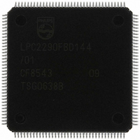
LPC2290FBD144/01,5 NXP Semiconductors, LPC2290FBD144/01,5 Datasheet - Page 7

LPC2290FBD144/01,5
Manufacturer Part Number
LPC2290FBD144/01,5
Description
IC ARM7 MCU RAM 16K 144-LQFP
Manufacturer
NXP Semiconductors
Series
LPC2200r
Datasheet
1.LPC2290FBD144015.pdf
(41 pages)
Specifications of LPC2290FBD144/01,5
Package / Case
144-LQFP
Core Processor
ARM7
Core Size
16/32-Bit
Speed
60MHz
Connectivity
CAN, EBI/EMI, I²C, Microwire, SPI, SSI, SSP, UART/USART
Peripherals
PWM, WDT
Number Of I /o
76
Program Memory Type
ROMless
Ram Size
64K x 8
Voltage - Supply (vcc/vdd)
1.65 V ~ 3.6 V
Data Converters
A/D 8x10b
Oscillator Type
Internal
Operating Temperature
-40°C ~ 85°C
Processor Series
LPC22
Core
ARM7TDMI-S
Data Bus Width
16 bit, 32 bit
Data Ram Size
64 KB
Interface Type
CAN/I2C/SPI/UART
Maximum Clock Frequency
72 MHz
Number Of Programmable I/os
76
Number Of Timers
2
Operating Supply Voltage
3.3 V
Maximum Operating Temperature
+ 85 C
Mounting Style
SMD/SMT
3rd Party Development Tools
MDK-ARM, RL-ARM, ULINK2
Minimum Operating Temperature
- 40 C
On-chip Adc
8-ch x 10-bit
Package
144LQFP
Device Core
ARM7TDMI-S
Family Name
LPC2000
Maximum Speed
72 MHz
Lead Free Status / RoHS Status
Lead free / RoHS Compliant
For Use With
OM10091 - KIT DEV PHYCORE-ARM7/LPC2220568-1757 - BOARD EVAL FOR LPC220X ARM MCU
Eeprom Size
-
Program Memory Size
-
Lead Free Status / Rohs Status
Lead free / RoHS Compliant
Other names
568-4013
935282079551
LPC2290FBD144/01-S
935282079551
LPC2290FBD144/01-S
Available stocks
Company
Part Number
Manufacturer
Quantity
Price
Company:
Part Number:
LPC2290FBD144/01,5
Manufacturer:
NXP Semiconductors
Quantity:
10 000
NXP Semiconductors
Table 3.
LPC2290_3
Product data sheet
Symbol
P0.19/MAT1.2/
MOSI1/CAP1.2
P0.20/MAT1.3/
SSEL1/EINT3
P0.21/PWM5/
CAP1.3
P0.22/CAP0.0/
MAT0.0
P0.23/RD2
P0.24/TD2
P0.25
P0.27/AIN0/
CAP0.1/MAT0.1
P0.28/AIN1/
CAP0.2/MAT0.2
P0.29/AIN2/
CAP0.3/MAT0.3
P0.30/AIN3/
EINT3/CAP0.0
P1.0 to P1.31
Pin description
Pin
122
123
4
5
6
8
21
23
25
32
33
[1]
[1]
[1]
[1]
[1]
[4]
[4]
[4]
[4]
[1]
[2]
…continued
Type
I/O
O
I/O
I
I/O
O
I
I
I/O
O
I
I/O
I
O
I/O
I
I/O
O
I/O
I
I/O
I
I
O
I/O
I
I
O
I/O
I
I
O
I/O
I
I
I
I/O
Description
P0.19 — General purpose digital input/output pin.
MAT1.2 — Match output for Timer 1, channel 2.
MOSI1 — Master Out Slave In for SPI1/SSP. Data output from SPI master or
data input to SPI slave (SSP is available in LPC2290/01 only).
CAP1.2 — Capture input for Timer 1, channel 2.
P0.20 — General purpose digital input/output pin.
MAT1.3 — Match output for Timer 1, channel 3.
SSEL1 — Slave Select for SPI1/SSP. Selects the SPI interface as a slave
(SSP is available in LPC2290/01 only).
EINT3 — External interrupt 3 input.
P0.21 — General purpose digital input/output pin.
PWM5 — Pulse Width Modulator output 5.
CAP1.3 — Capture input for Timer 1, channel 3.
P0.22 — General purpose digital input/output pin.
CAP0.0 — Capture input for Timer 0, channel 0.
MAT0.0 — Match output for Timer 0, channel 0.
P0.23 — General purpose digital input/output pin.
RD2 — CAN2 receiver input.
P0.24 — General purpose digital input/output pin.
TD2 — CAN2 transmitter output.
P0.25 — General purpose digital input/output pin.
RD1 — CAN1 receiver input.
P0.27 — General purpose digital input/output pin.
AIN0 — ADC, input 0. This analog input is always connected to its pin.
CAP0.1 — Capture input for Timer 0, channel 1.
MAT0.1 — Match output for Timer 0, channel 1.
P0.28 — General purpose digital input/output pin.
AIN1 — ADC, input 1. This analog input is always connected to its pin.
CAP0.2 — Capture input for Timer 0, channel 2.
MAT0.2 — Match output for Timer 0, channel 2.
P0.29 — General purpose digital input/output pin.
AIN2 — ADC, input 2. This analog input is always connected to its pin.
CAP0.3 — Capture input for Timer 0, Channel 3.
MAT0.3 — Match output for Timer 0, channel 3.
P0.30 — General purpose digital input/output pin.
AIN3 — ADC, input 3. This analog input is always connected to its pin.
EINT3 — External interrupt 3 input.
CAP0.0 — Capture input for Timer 0, channel 0.
Port 1: Port 1 is a 32-bit bidirectional I/O port with individual direction controls
for each bit. The operation of port 1 pins depends upon the pin function
selected via the Pin Connect Block.
Pins 2 through 15 of port 1 are not available.
Rev. 03 — 16 November 2006
16/32-bit ARM microcontroller with external memory interface
LPC2290
© NXP B.V. 2006. All rights reserved.
7 of 41


