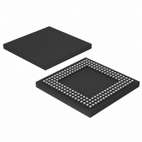
LPC2880FET180,551 NXP Semiconductors, LPC2880FET180,551 Datasheet - Page 11

LPC2880FET180,551
Manufacturer Part Number
LPC2880FET180,551
Description
IC ARM7 MCU RAM 16K 180TFBGA
Manufacturer
NXP Semiconductors
Series
LPC2800r
Datasheet
1.LPC2880FET180551.pdf
(43 pages)
Specifications of LPC2880FET180,551
Core Processor
ARM7
Core Size
16/32-Bit
Speed
60MHz
Connectivity
EBI/EMI, I²C, IrDA, MMC, UART/USART, USB
Peripherals
DMA, I²S, LCD, WDT
Number Of I /o
85
Program Memory Type
ROMless
Ram Size
64K x 8
Voltage - Supply (vcc/vdd)
1.7 V ~ 3.6 V
Data Converters
A/D 5x10b
Oscillator Type
External
Operating Temperature
-40°C ~ 85°C
Package / Case
180-TFBGA
Processor Series
LPC28
Core
ARM7TDMI-S
Data Bus Width
32 bit
Data Ram Size
64 KB
Interface Type
I2C, I2S, UART, USB
Maximum Clock Frequency
60 MHz
Number Of Programmable I/os
81
Number Of Timers
2
Operating Supply Voltage
3.3 V
Maximum Operating Temperature
+ 85 C
Mounting Style
SMD/SMT
3rd Party Development Tools
MDK-ARM, RL-ARM, ULINK2
Minimum Operating Temperature
- 40 C
On-chip Adc
10 bit, 5 Channel
For Use With
OM10092 - EVAL BOARD FOR LPC288X
Lead Free Status / RoHS Status
Lead free / RoHS Compliant
Eeprom Size
-
Program Memory Size
-
Lead Free Status / Rohs Status
Details
Other names
568-3245
935281368551
LPC2880FET180-S
935281368551
LPC2880FET180-S
Available stocks
Company
Part Number
Manufacturer
Quantity
Price
Company:
Part Number:
LPC2880FET180,551
Manufacturer:
NXP Semiconductors
Quantity:
10 000
NXP Semiconductors
Table 4.
[1]
6. Functional description
LPC2880_LPC2888_3
Preliminary data sheet
Symbol
Digital power and ground
V
V
V
V
V
V
V
V
V
V
V
V
V
V
V
V
V
V
V
V
V
V
V
V
V
V
DD1(CORE1V8)
DD1(FLASH1V8)
DD1(EMC)
DD1(IO3V3)
DD2(CORE1V8)
DD2(EMC)
DD2(FLASH1V8)
DD2(IO3V3)
DD3(IO3V3)
DD4(IO3V3)
DD5(IO3V3)
DD6(IO3V3)
SS1(CORE)
SS1(EMC)
SS1(INT)
SS1(IO)
SS2(CORE)
SS2(EMC)
SS2(INT)
SS2(IO)
SS3(CORE)
SS3(INT)
SS3(IO)
SS4(IO)
SS5(IO)
SS6(IO)
I = input; O = output; I/O = input/output; RV = reference voltage; FI = functional input; FO = functional output; P = power or ground
Pin description
6.1 Architectural overview
Ball #
H1
V15
A16
E1
V11
A7
V16
V5
V14
J18
R1
R2
G1
A15
T12
F1
V12
A6
U11
V6
V17
T11
V13
H18
P2
P1
The LPC2880/2888 includes an ARM7TDMI CPU with an 8 kB cache, an AMBA AHB
interfacing to high-speed on-chip peripherals and internal and external memory, and four
AMBA APBs for connection to other on-chip peripheral functions.
The LPC2880/2888 includes a multi-layer AHB and four separate APBs, in order to
minimize interference between the USB controller, other DMA operations, and processor
activity. Bus masters include the ARM7 itself, the USB block, and the general purpose
DMA controller.
…continued
Type
P
P
P
P
P
P
P
P
P
P
P
P
P
P
P
P
P
P
P
P
P
P
P
P
P
P
[1]
Description
1.8 V for internal RAM and ROM
1.8 V for internal flash memory
1.8 V or 3.3 V for external memory controller
3.3 V for peripherals
1.8 V for core
1.8 V or 3.3 V for external memory controller
1.8 V for internal flash memory
3.3 V for peripherals
3.3 V for peripherals
3.3 V for peripherals
3.3 V for peripherals
3.3 V for peripherals
ground for internal RAM and ROM
ground for external memory controller
ground for other internal blocks
ground for peripherals
ground for core
ground for external memory controller
ground for other internal blocks
ground for peripherals
ground for core, substrate, flash
ground for other internal blocks
ground for peripherals
ground for peripherals
ground for peripherals
ground for peripherals
16/32-bit ARM microcontrollers with external memory interface
Rev. 03 — 17 April 2008
LPC2880; LPC2888
© NXP B.V. 2008. All rights reserved.
11 of 43


