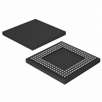
LPC2880FET180,551 NXP Semiconductors, LPC2880FET180,551 Datasheet - Page 30

LPC2880FET180,551
Manufacturer Part Number
LPC2880FET180,551
Description
IC ARM7 MCU RAM 16K 180TFBGA
Manufacturer
NXP Semiconductors
Series
LPC2800r
Datasheet
1.LPC2880FET180551.pdf
(43 pages)
Specifications of LPC2880FET180,551
Core Processor
ARM7
Core Size
16/32-Bit
Speed
60MHz
Connectivity
EBI/EMI, I²C, IrDA, MMC, UART/USART, USB
Peripherals
DMA, I²S, LCD, WDT
Number Of I /o
85
Program Memory Type
ROMless
Ram Size
64K x 8
Voltage - Supply (vcc/vdd)
1.7 V ~ 3.6 V
Data Converters
A/D 5x10b
Oscillator Type
External
Operating Temperature
-40°C ~ 85°C
Package / Case
180-TFBGA
Processor Series
LPC28
Core
ARM7TDMI-S
Data Bus Width
32 bit
Data Ram Size
64 KB
Interface Type
I2C, I2S, UART, USB
Maximum Clock Frequency
60 MHz
Number Of Programmable I/os
81
Number Of Timers
2
Operating Supply Voltage
3.3 V
Maximum Operating Temperature
+ 85 C
Mounting Style
SMD/SMT
3rd Party Development Tools
MDK-ARM, RL-ARM, ULINK2
Minimum Operating Temperature
- 40 C
On-chip Adc
10 bit, 5 Channel
For Use With
OM10092 - EVAL BOARD FOR LPC288X
Lead Free Status / RoHS Status
Lead free / RoHS Compliant
Eeprom Size
-
Program Memory Size
-
Lead Free Status / Rohs Status
Details
Other names
568-3245
935281368551
LPC2880FET180-S
935281368551
LPC2880FET180-S
Available stocks
Company
Part Number
Manufacturer
Quantity
Price
Company:
Part Number:
LPC2880FET180,551
Manufacturer:
NXP Semiconductors
Quantity:
10 000
NXP Semiconductors
Table 6.
T
[1]
[2]
[3]
[4]
[5]
[6]
[7]
[8]
[9]
[10] Applies to 5 V tolerant pins.
[11] Accounts for 100 mV voltage drop in all supply lines.
[12] Only allowed for a short time period.
[13] Applies to pins V
[14] Applies to pins V
[15] Applies to pin V
[16] Applies to pin V
[17] Applies to pin V
[18] Applies to pins V
[19] Applies to pin V
[20] All the above tests were done on the Icetech LPC288x evaluation board. Here are the different configurations that need to be done to
LPC2880_LPC2888_3
Preliminary data sheet
Symbol
I
I
I
DD
DD
DD
amb
Typical ratings are not guaranteed. The values listed are at room temperature (+25 ˚C), nominal supply voltages.
Applies to pins V
V
External supply voltage; applies to pins V
Applies to pins V
External supply voltage; applies to pins V
Referenced to the applicable V
Including voltage on outputs in 3-state mode.
Applies to pins with a V
Applies to pins with a V
achieve the above numbers:
a) Resistors R7 and R8 on the board should be removed to reduce the power consumption on the LED’s D2 and D3.
b) The Analog-to-Digital Converter (ADC), the Dual-channel 16-bit Analog-to-Digital Converter and the Dual-channel 16-bit
c) The USB device controller is suspended.
d) All power control registers in the Clock Generation Unit have a value of 7h, and the Power Mode register in the Clock Generation Unit
e) The floating pins are set to output state.
f) The Event Router is configured in such a way that it will generate its wake-up output to the Clock Generation Unit with a rising-edge
= 40 C to +85 C, unless otherwise specified.
DD2(USB1V8)
Digital-to-Analog Converter are powered down.
has a value of 3h such that the output clocks of all spreading stages are disabled.
signal on the MODE1/P2[2] or the MODE2/P2[3].
Static characteristics
Parameter
supply current
supply current
supply current
.
DD(OSC1V8)
DD(OSC321V8)
DD(ADC3V3)
DD(DAC3V3)
DD1(CORE1V8)
DD(DADC3V3)
DD1(CORE1V8)
DD1(EMC)
DD(DADC1V8)
DD
DD
, V
.
.
.
supply of 1.8 V.
supply of 3.3 V.
.
DD2(EMC)
, V
, V
, V
, V
DD
DD(ADC3V3)
DD(DADC3V3)
DD2(CORE1V8)
DD2(CORE1V8)
for the pin, which must be present.
…continued
.
DD3(USB3V3)
, V
DD1(EMC)
.
DD(DAC3V3)
, V
, V
DD(DADC1V8)
DD1(FLASH1V8)
Conditions
32.768 kHz oscillator stops;
12 MHz oscillator runs;
external DC-to-DC
converter supplies 1.8 V
32.768 kHz oscillator runs;
12 MHz oscillator stops;
external DC-to-DC
converter supplies 3.3 V
32.768 kHz oscillator stops;
12 MHz oscillator runs;
external DC-to-DC
converter supplies 3.3 V
, V
16/32-bit ARM microcontrollers with external memory interface
, V
DD2(EMC)
Rev. 03 — 17 April 2008
, V
DD4(USB3V3)
DD5(IO3V3)
, V
, V
.
DD1(FLASH1V8)
DD2(FLASH1V8)
, V
, V
DD1(IO3V3)
DD6(IO3V3)
, V
DD2(FLASH1V8)
, V
.
DD2(IO3V3)
LPC2880; LPC2888
[20]
[20]
[20]
, V
, V
Min
-
-
-
DD(OSC1V8)
DD3(IO3V3)
, V
, V
DD4(IO3V3)
Typ
0.97
1.27
1.27
DD(OSC321V8)
[1]
© NXP B.V. 2008. All rights reserved.
.
Max
-
-
-
, V
DD1(USB1V8)
30 of 43
Unit
mA
mA
mA
,


