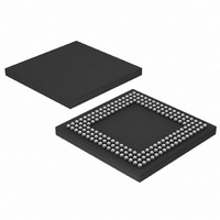
LPC2880FET180,551 NXP Semiconductors, LPC2880FET180,551 Datasheet - Page 20

LPC2880FET180,551
Manufacturer Part Number
LPC2880FET180,551
Description
IC ARM7 MCU RAM 16K 180TFBGA
Manufacturer
NXP Semiconductors
Series
LPC2800r
Datasheet
1.LPC2880FET180551.pdf
(43 pages)
Specifications of LPC2880FET180,551
Core Processor
ARM7
Core Size
16/32-Bit
Speed
60MHz
Connectivity
EBI/EMI, I²C, IrDA, MMC, UART/USART, USB
Peripherals
DMA, I²S, LCD, WDT
Number Of I /o
85
Program Memory Type
ROMless
Ram Size
64K x 8
Voltage - Supply (vcc/vdd)
1.7 V ~ 3.6 V
Data Converters
A/D 5x10b
Oscillator Type
External
Operating Temperature
-40°C ~ 85°C
Package / Case
180-TFBGA
Processor Series
LPC28
Core
ARM7TDMI-S
Data Bus Width
32 bit
Data Ram Size
64 KB
Interface Type
I2C, I2S, UART, USB
Maximum Clock Frequency
60 MHz
Number Of Programmable I/os
81
Number Of Timers
2
Operating Supply Voltage
3.3 V
Maximum Operating Temperature
+ 85 C
Mounting Style
SMD/SMT
3rd Party Development Tools
MDK-ARM, RL-ARM, ULINK2
Minimum Operating Temperature
- 40 C
On-chip Adc
10 bit, 5 Channel
For Use With
OM10092 - EVAL BOARD FOR LPC288X
Lead Free Status / RoHS Status
Lead free / RoHS Compliant
Eeprom Size
-
Program Memory Size
-
Lead Free Status / Rohs Status
Details
Other names
568-3245
935281368551
LPC2880FET180-S
935281368551
LPC2880FET180-S
Available stocks
Company
Part Number
Manufacturer
Quantity
Price
Company:
Part Number:
LPC2880FET180,551
Manufacturer:
NXP Semiconductors
Quantity:
10 000
NXP Semiconductors
LPC2880_LPC2888_3
Preliminary data sheet
6.14.1 Features
6.15.1 Features
6.14 UART and IrDA
6.15 I
The LPC2880/2888 contains one UART with baud rate generator and IrDA support.
The LPC2880/2888 I
master Transmit mode, master Receive mode, slave Transmit mode and slave Receive
mode. The interface complies with the entire I
power off to the LPC2880/2888 without causing a problem with other devices on the same
I
2
2
•
•
•
•
•
•
•
•
•
•
•
•
•
•
•
•
•
C-bus.
•
•
•
•
C-bus interface
The GPDMA supports a subset of the flow control signals supported by ARM DMA
channels, specifically ‘single’ but not ‘burst’ operation.
Memory-to-memory, memory-to-peripheral, peripheral-to-memory, and
peripheral-to-peripheral transfers.
Scatter or gather DMA is supported through the use of linked lists. This means that
the source and destination areas do not have to occupy contiguous areas of memory.
Rotating channel priority. Each DMA channel has equal opportunity to perform
transfers.
The GPDMA is one of three AHB masters in the LPC2880/2888, the others being the
ARM7 processor and the USB interface.
Incrementing or non-incrementing addressing for source and destination.
Supports 8 bit, 16 bit, and 32 bit wide transactions.
GPDMA channels can be programmed to swap data between big- and little-endian
formats during a transfer.
An interrupt to the processor can be generated on DMA completion, when a DMA
channel is halfway to completion, or when a DMA error has occurred.
32-Byte Receive and Transmit FIFOs.
Register locations conform to the 16C650 industry standard.
Receiver FIFO trigger points at 1 B, 16 B, 24 B, and 28 B.
Built-in baud rate generator.
CGU generates UART clock including fractional divider capability.
Auto baud capability.
Optional hardware flow control.
IrDA mode for infrared communication.
Standard I
Arbitration between simultaneously transmitting masters without corruption of serial
data on the bus.
Programmable clock allows adjustment of I
Bidirectional data transfer between masters and slaves.
2
C-bus interface, configurable as Master, Slave, or Master/Slave.
2
C-bus interface is byte oriented and has four operating modes:
16/32-bit ARM microcontrollers with external memory interface
Rev. 03 — 17 April 2008
2
C-bus specification , and allows turning
2
C-bus transfer rates.
LPC2880; LPC2888
© NXP B.V. 2008. All rights reserved.
20 of 43


