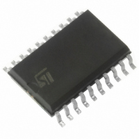
ST7FDALIF2M6 STMicroelectronics, ST7FDALIF2M6 Datasheet - Page 110

ST7FDALIF2M6
Manufacturer Part Number
ST7FDALIF2M6
Description
IC MCU 8BIT 8K 20-SOIC
Manufacturer
STMicroelectronics
Series
ST7r
Datasheet
1.ST7DALI-EVAL.pdf
(171 pages)
Specifications of ST7FDALIF2M6
Core Processor
ST7
Core Size
8-Bit
Speed
8MHz
Connectivity
DALI, SPI
Peripherals
LVD, POR, PWM, WDT
Number Of I /o
15
Program Memory Size
8KB (8K x 8)
Program Memory Type
FLASH
Eeprom Size
256 x 8
Ram Size
384 x 8
Voltage - Supply (vcc/vdd)
2.4 V ~ 5.5 V
Data Converters
A/D 7x10b
Oscillator Type
Internal
Operating Temperature
-40°C ~ 85°C
Package / Case
20-SOIC (7.5mm Width)
Processor Series
ST7DALI
Core
ST7
Data Bus Width
8 bit
Data Ram Size
384 B
Interface Type
DALI, SPI
Maximum Clock Frequency
8 MHz
Number Of Programmable I/os
15
Number Of Timers
4 bit
Operating Supply Voltage
2.4 V to 5.5 V
Maximum Operating Temperature
+ 85 C
Mounting Style
SMD/SMT
Development Tools By Supplier
ST7FLITE-SK/RAIS, ST7DALI-EVAL, ST7MDT10-DVP3, ST7MDT10-EMU3, STX-RLINK
Minimum Operating Temperature
- 40 C
On-chip Adc
8 bit
For Use With
497-5046 - KIT TOOL FOR ST7/UPSD/STR7 MCU
Lead Free Status / RoHS Status
Lead free / RoHS Compliant
Other names
497-2131-5
Available stocks
Company
Part Number
Manufacturer
Quantity
Price
Company:
Part Number:
ST7FDALIF2M6TR
Manufacturer:
NEC
Quantity:
670
Serial peripheral interface (SPI)
Note:
Note:
Note:
17.7.2
110/171
Bit 4 = MSTR Master Mode.
This bit is set and cleared by software. It is also cleared by hardware when, in master mode,
SS=0 (see
0: Slave mode
1: Master mode. The function of the SCK pin changes from an input to an output and the
functions of the MISO and MOSI pins are reversed.
Bit 3 = CPOL Clock Polarity.
This bit is set and cleared by software. This bit determines the idle state of the serial Clock.
The CPOL bit affects both the master and slave modes.
0: SCK pin has a low level idle state
1: SCK pin has a high level idle state
If CPOL is changed at the communication byte boundaries, the SPI must be disabled by
resetting the SPE bit.
Bit 2 = CPHA Clock Phase.
This bit is set and cleared by software.
0: The first clock transition is the first data capture edge.
1: The second clock transition is the first capture edge.
The slave must have the same CPOL and CPHA settings as the master.
Bits 1:0 = SPR[1:0] Serial Clock Frequency.
These bits are set and cleared by software. Used with the SPR2 bit, they select the baud
rate of the SPI serial clock SCK output by the SPI in master mode.
These 2 bits have no effect in slave mode.
Table 48.
Control/status register (SPICSR)
Read/Write (some bits Read Only)
Reset Value: 0000 0000 (00h)
Bit 7 = SPIF Serial Peripheral Data Transfer Flag (Read only).
This bit is set by hardware when a transfer has been completed. An interrupt is generated if
SPIF
7
Master mode fault (MODF) on page
SPI master mode SCK frequency
Serial clock
WCOL
f
f
f
f
CPU
f
f
CPU
CPU
CPU
CPU
CPU
/128
/16
/32
/64
/4
/8
OVR
MODF
SPR2
105).
1
0
0
1
0
0
-
SOD
SPR1
0
0
0
1
1
1
SSM
ST7DALIF2
SPR0
0
0
1
0
0
1
SSI
0


