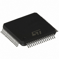
ST72F521AR9TC STMicroelectronics, ST72F521AR9TC Datasheet - Page 182

ST72F521AR9TC
Manufacturer Part Number
ST72F521AR9TC
Description
IC MCU 8BIT 60K FLASH 64-TQFP
Manufacturer
STMicroelectronics
Series
ST7r
Datasheet
1.ST72F521M9T6.pdf
(215 pages)
Specifications of ST72F521AR9TC
Core Processor
ST7
Core Size
8-Bit
Speed
8MHz
Connectivity
CAN, I²C, SCI, SPI
Peripherals
LVD, POR, PWM, WDT
Number Of I /o
48
Program Memory Size
60KB (60K x 8)
Program Memory Type
FLASH
Ram Size
2K x 8
Voltage - Supply (vcc/vdd)
3.8 V ~ 5.5 V
Data Converters
A/D 16x10b
Oscillator Type
Internal
Operating Temperature
-40°C ~ 125°C
Package / Case
64-TQFP, 64-VQFP
For Use With
497-6453 - BOARD EVAL BASED ON ST7LNBX
Lead Free Status / RoHS Status
Lead free / RoHS Compliant
Eeprom Size
-
Available stocks
Company
Part Number
Manufacturer
Quantity
Price
Company:
Part Number:
ST72F521AR9TC
Manufacturer:
STMicroelectronics
Quantity:
10 000
Company:
Part Number:
ST72F521AR9TCE
Manufacturer:
STMicroelectronics
Quantity:
10 000
Company:
Part Number:
ST72F521AR9TCTR
Manufacturer:
STMicroelectronics
Quantity:
10 000
ST72F521, ST72521B
12.8 I/O PORT PIN CHARACTERISTICS
12.8.1 General Characteristics
Subject to general operating conditions for V
Figure 95. Unused I/O Pins configured as input
Notes:
1. Data based on characterization results, not tested in production.
2. Hysteresis voltage between Schmitt trigger switching levels. Based on characterization results, not tested.
3. When the current limitation is not possible, the V
tion. A positive injection is induced by V
on page 166
4. Configuration not recommended, all unused pins must be kept at a fixed voltage: using the output mode of the I/O for
example and leaving the I/O unconnected on the board or an external pull-up or pull-down resistor (see
based on design simulation and/or technology characteristics, not tested in production.
5. The R
scribed in
6. To generate an external interrupt, a minimum pulse width has to be applied on an I/O port pin configured as an external
interrupt source.
182/215
ΣI
I
Symbol
INJ(PIN)
t
t
INJ(PIN)
Note: I/O can be left unconnected if it is configured as output
(0 or 1) by the software. This has the advantage of
greater EMC robustness and lower cost.
t
f(IO)out
r(IO)out
w(IT)in
V
V
R
C
V
V
V
V
I
I
hys
hys
PU
S
IH
IH
L
IO
IL
IL
3)
PU
3)
Figure
Input low level voltage
Input high level voltage
Schmitt trigger voltage hysteresis
Input low level voltage
Input high level voltage
Schmitt trigger voltage hysteresis
Injected Current on PC6 (Flash de-
vices only)
Injected Current on an I/O pin
Total injected current (sum of all I/O
and control pins)
Input leakage current
Static current consumption
Weak pull-up equivalent resistor
I/O pin capacitance
Output high to low level fall time
Output low to high level rise time
External interrupt pulse time
pull-up equivalent resistor is based on a resistive transistor (corresponding I
for more details.
96).
V
DD
Parameter
10kΩ
10kΩ
UNUSED I/O PORT
UNUSED I/O PORT
1)
1)
1)
1)
IN
6)
>V
ST7XXX
ST7XXX
DD
5)
1)
1)
2)
2)
while a negative injection is induced by V
CMOS ports
TTL ports
V
V
Floating input mode
V
C
Between 10% and 90%
IN
DD
DD
SS
IN
L
=50pF
=
maximum must be respected, otherwise refer to I
≤
=5V
, f
V
V
SS
OSC
IN
Conditions
≤
V
, and T
DD
Figure 96. Typical I
V
DD
=5V
A
4)
unless otherwise specified.
90
80
70
60
50
40
30
20
10
0
2
0.7xV
2.5
Min
50
2
0
1
Ta=140°C
Ta=95°C
Ta=25°C
Ta=-45°C
DD
3
PU
3.5
IN
vs. V
PU
<V
V dd(V)
Typ
400
120
0.7
25
25
1
5
4
SS
current characteristics de-
DD
. Refer to
4.5
with V
0.3xV
5
± 25
Max
250
0.8
± 4
INJ(PIN)
+4
±1
Figure
5.5
section 12.2.2
DD
IN
=V
specifica-
6
95). Data
SS
t
Unit
mA
CPU
µA
kΩ
pF
ns
V


