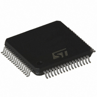
ST72F521AR9TC STMicroelectronics, ST72F521AR9TC Datasheet - Page 27

ST72F521AR9TC
Manufacturer Part Number
ST72F521AR9TC
Description
IC MCU 8BIT 60K FLASH 64-TQFP
Manufacturer
STMicroelectronics
Series
ST7r
Datasheet
1.ST72F521M9T6.pdf
(215 pages)
Specifications of ST72F521AR9TC
Core Processor
ST7
Core Size
8-Bit
Speed
8MHz
Connectivity
CAN, I²C, SCI, SPI
Peripherals
LVD, POR, PWM, WDT
Number Of I /o
48
Program Memory Size
60KB (60K x 8)
Program Memory Type
FLASH
Ram Size
2K x 8
Voltage - Supply (vcc/vdd)
3.8 V ~ 5.5 V
Data Converters
A/D 16x10b
Oscillator Type
Internal
Operating Temperature
-40°C ~ 125°C
Package / Case
64-TQFP, 64-VQFP
For Use With
497-6453 - BOARD EVAL BASED ON ST7LNBX
Lead Free Status / RoHS Status
Lead free / RoHS Compliant
Eeprom Size
-
Available stocks
Company
Part Number
Manufacturer
Quantity
Price
Company:
Part Number:
ST72F521AR9TC
Manufacturer:
STMicroelectronics
Quantity:
10 000
Company:
Part Number:
ST72F521AR9TCE
Manufacturer:
STMicroelectronics
Quantity:
10 000
Company:
Part Number:
ST72F521AR9TCTR
Manufacturer:
STMicroelectronics
Quantity:
10 000
RESET SEQUENCE MANAGER (Cont’d)
The RESET pin is an asynchronous signal which
plays a major role in EMS performance. In a noisy
environment, it is recommended to follow the
guidelines mentioned in the electrical characteris-
tics section.
If the external RESET pulse is shorter than
t
signal on the RESET pin may be stretched. Other-
wise the delay will not be applied (see long ext.
Reset in
SET pulse recognition, the device RESET pin acts
as an output that is pulled low during at least
t
6.3.3 External Power-On RESET
If the LVD is disabled by option byte, to start up the
microcontroller correctly, the user must ensure by
means of an external reset circuit that the reset
signal is held low until V
level specified for the selected f
(see
Figure 14. RESET Sequences
w(RSTL)out
w(RSTL)out
WATCHDOG
RESET
EXTERNAL
RESET
SOURCE
RESET PIN
“OPERATING CONDITIONS” on page
V
V
IT+(LVD)
IT-(LVD)
Figure
.
(see short ext. Reset in
V
RUN
14). Starting from the external RE-
DD
ACTIVE PHASE
DD
RESET
LVD
is over the minimum
OSC
Figure
t
t
frequency.
w(RSTL)out
h(RSTL)in
RUN
14), the
167)
ACTIVE
PHASE
SHORT EXT.
RESET
DELAY
A proper reset signal for a slow rising V
can generally be provided by an external RC net-
work connected to the RESET pin.
6.3.4 Internal Low Voltage Detector (LVD)
RESET
Two different RESET sequences caused by the in-
ternal LVD circuitry can be distinguished:
■
■
The device RESET pin acts as an output that is
pulled low when V
V
The LVD filters spikes on V
avoid parasitic resets.
6.3.5 Internal Watchdog RESET
The RESET sequence generated by a internal
Watchdog counter overflow is shown in
Starting from the Watchdog counter underflow, the
device RESET pin acts as an output that is pulled
low during at least t
DD
t
Power-On RESET
Voltage Drop RESET
h(RSTL)in
t
w(RSTL)out
<V
RUN
IT-
(falling edge) as shown in
WATCHDOG UNDERFLOW
ACTIVE
PHASE
LONG EXT.
RESET
w(RSTL)out
DD
ST72F521, ST72521B
<V
INTERNAL RESET (256 or 4096 T
VECTOR FETCH
RUN
DD
IT+
.
larger than t
ACTIVE
(rising edge) or
PHASE
WATCHDOG
RESET
t
w(RSTL)out
Figure
Figure
DD
g(VDD)
14.
supply
RUN
27/215
CPU
14.
to
)


