MC908GR4CDWE Freescale Semiconductor, MC908GR4CDWE Datasheet - Page 206
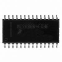
MC908GR4CDWE
Manufacturer Part Number
MC908GR4CDWE
Description
IC MCU 4K FLASH 8MHZ 28-SOIC
Manufacturer
Freescale Semiconductor
Series
HC08r
Specifications of MC908GR4CDWE
Core Processor
HC08
Core Size
8-Bit
Speed
8MHz
Connectivity
SCI, SPI
Peripherals
LVD, POR, PWM
Number Of I /o
17
Program Memory Size
4KB (4K x 8)
Program Memory Type
FLASH
Ram Size
384 x 8
Voltage - Supply (vcc/vdd)
2.7 V ~ 5.5 V
Data Converters
A/D 6x8b
Oscillator Type
Internal
Operating Temperature
-40°C ~ 85°C
Package / Case
28-SOIC (7.5mm Width)
Controller Family/series
HC08
No. Of I/o's
21
Ram Memory Size
384Byte
Cpu Speed
8MHz
No. Of Timers
1
Embedded Interface Type
I2C, SCI, SPI
Rohs Compliant
Yes
Processor Series
HC08GR
Core
HC08
Data Bus Width
8 bit
Data Ram Size
384 B
Interface Type
SCI, SPI
Maximum Clock Frequency
8.2 MHz
Number Of Programmable I/os
21
Number Of Timers
3
Maximum Operating Temperature
+ 85 C
Mounting Style
SMD/SMT
Development Tools By Supplier
FSICEBASE, DEMO908GZ60E, M68CBL05CE, M68EML08GPGTE
Minimum Operating Temperature
- 40 C
On-chip Adc
8 bit, 6 Channel
Lead Free Status / RoHS Status
Lead free / RoHS Compliant
Eeprom Size
-
Lead Free Status / Rohs Status
Details


Serial Peripheral Interface (SPI)
20.3 Pin Name Conventions and I/O Register Addresses
The text that follows describes the SPI. The SPI I/O pin names are SS (slave select), SPSCK (SPI serial
clock), MOSI (master out slave in), and MISO (master in/slave out). The SPI shares four I/O pins with four
parallel I/O ports.
The full names of the SPI I/O pins are shown in
follows.
20.4 Functional Description
Figure 20-1
The SPI module allows full-duplex, synchronous, serial communication between the MCU and peripheral
devices, including other MCUs. Software can poll the SPI status flags or SPI operation can be
interrupt-driven.
If a port bit is configured for input, then an internal pullup device may be enabled for that port bit. See
16.5.3 Port D Input Pullup Enable
The following paragraphs describe the operation of the SPI module.
206
Addr.
$0010
$0011
$0012
Register Name
SPI Status and Control
summarizes the SPI I/O registers and
SPI Control Register
Register (SPSCR)
Pin Names:
SPI Data Register
Full SPI
SPI Generic
Pin Names:
(SPCR)
(SPDR)
SPI
Reset:
Reset:
Reset:
Read:
Read:
Read:
Write:
Write:
Write:
MC68HC908GR8 • MC68HC908GR4 Data Sheet, Rev. 7
Figure 20-1. SPI I/O Register Summary
PTD1/ATD9
Table 20-1. Pin Name Conventions
Register.
SPRIE
MISO
Bit 7
SPRF
R7
T7
0
0
= Unimplemented
ERRIE
PTD2/ATD10
R6
T6
6
R
0
0
Table
MOSI
Figure 20-2
SPMSTR
OVRF
20-1. The generic pin names appear in the text that
R5
T5
5
1
0
PTD0/ATD8
MODF
CPOL
Unaffected by reset
SS
shows the structure of the SPI module.
R4
T4
4
R
0
0
= Reserved
PTD3/ATD11
CPHA
SPTE
R3
T3
3
1
1
SPSCK
MODFEN
SPWOM
R2
T2
2
0
0
Freescale Semiconductor
CGND
V
SS
SPR1
SPE
R1
T1
1
0
0
SPTIE
Bit 0
SPR0
R0
T0
0
0
Related parts for MC908GR4CDWE
Image
Part Number
Description
Manufacturer
Datasheet
Request
R

Part Number:
Description:
Manufacturer:
Freescale Semiconductor, Inc
Datasheet:
Part Number:
Description:
Manufacturer:
Freescale Semiconductor, Inc
Datasheet:
Part Number:
Description:
Manufacturer:
Freescale Semiconductor, Inc
Datasheet:
Part Number:
Description:
Manufacturer:
Freescale Semiconductor, Inc
Datasheet:
Part Number:
Description:
Manufacturer:
Freescale Semiconductor, Inc
Datasheet:
Part Number:
Description:
Manufacturer:
Freescale Semiconductor, Inc
Datasheet:
Part Number:
Description:
Manufacturer:
Freescale Semiconductor, Inc
Datasheet:
Part Number:
Description:
Manufacturer:
Freescale Semiconductor, Inc
Datasheet:
Part Number:
Description:
Manufacturer:
Freescale Semiconductor, Inc
Datasheet:
Part Number:
Description:
Manufacturer:
Freescale Semiconductor, Inc
Datasheet:
Part Number:
Description:
Manufacturer:
Freescale Semiconductor, Inc
Datasheet:
Part Number:
Description:
Manufacturer:
Freescale Semiconductor, Inc
Datasheet:
Part Number:
Description:
Manufacturer:
Freescale Semiconductor, Inc
Datasheet:
Part Number:
Description:
Manufacturer:
Freescale Semiconductor, Inc
Datasheet:
Part Number:
Description:
Manufacturer:
Freescale Semiconductor, Inc
Datasheet: