MC908GR4CDWE Freescale Semiconductor, MC908GR4CDWE Datasheet - Page 280
MC908GR4CDWE
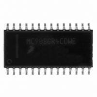
Manufacturer Part Number
MC908GR4CDWE
Description
IC MCU 4K FLASH 8MHZ 28-SOIC
Manufacturer
Freescale Semiconductor
Series
HC08r
Specifications of MC908GR4CDWE
Core Processor
HC08
Core Size
8-Bit
Speed
8MHz
Connectivity
SCI, SPI
Peripherals
LVD, POR, PWM
Number Of I /o
17
Program Memory Size
4KB (4K x 8)
Program Memory Type
FLASH
Ram Size
384 x 8
Voltage - Supply (vcc/vdd)
2.7 V ~ 5.5 V
Data Converters
A/D 6x8b
Oscillator Type
Internal
Operating Temperature
-40°C ~ 85°C
Package / Case
28-SOIC (7.5mm Width)
Controller Family/series
HC08
No. Of I/o's
21
Ram Memory Size
384Byte
Cpu Speed
8MHz
No. Of Timers
1
Embedded Interface Type
I2C, SCI, SPI
Rohs Compliant
Yes
Processor Series
HC08GR
Core
HC08
Data Bus Width
8 bit
Data Ram Size
384 B
Interface Type
SCI, SPI
Maximum Clock Frequency
8.2 MHz
Number Of Programmable I/os
21
Number Of Timers
3
Maximum Operating Temperature
+ 85 C
Mounting Style
SMD/SMT
Development Tools By Supplier
FSICEBASE, DEMO908GZ60E, M68CBL05CE, M68EML08GPGTE
Minimum Operating Temperature
- 40 C
On-chip Adc
8 bit, 6 Channel
Lead Free Status / RoHS Status
Lead free / RoHS Compliant
Eeprom Size
-
Lead Free Status / Rohs Status
Details


System Integration Module (SIM)
19.4.2.3 Illegal Opcode Reset
19.4.2.4 Illegal Address Reset
19.4.2.5 Low-Voltage Inhibit (LVI) Reset
Technical Data
280
The COP module is disabled if the RST pin or the IRQ pin is held at V
while the MCU is in monitor mode. The COP module can be disabled
only through combinational logic conditioned with the high voltage signal
on the RST or the IRQ pin. This prevents the COP from becoming
disabled as a result of external noise. During a break state, V
RST pin disables the COP module.
The SIM decodes signals from the CPU to detect illegal instructions. An
illegal instruction sets the ILOP bit in the SIM reset status register
(SRSR) and causes a reset.
If the stop enable bit, STOP, in the mask option register is logic 0, the
SIM treats the STOP instruction as an illegal opcode and causes an
illegal opcode reset. The SIM actively pulls down the RST pin for all
internal reset sources.
An opcode fetch from an unmapped address generates an illegal
address reset. The SIM verifies that the CPU is fetching an opcode prior
to asserting the ILAD bit in the SIM reset status register (SRSR) and
resetting the MCU. A data fetch from an unmapped address does not
generate a reset. The SIM actively pulls down the RST pin for all internal
reset sources.
The low-voltage inhibit module (LVI) asserts its output to the SIM when
the V
status register (SRSR) is set, and the external reset pin (RST) is held low
while the SIM counter counts out 4096 CGMXCLK cycles. Sixty-four
CGMXCLK cycles later, the CPU is released from reset to allow the reset
vector sequence to occur. The SIM actively pulls down the RST pin for
all internal reset sources.
Freescale Semiconductor, Inc.
For More Information On This Product,
DD
voltage falls to the LVI
System Integration Module (SIM)
Go to: www.freescale.com
TRIPF
voltage. The LVI bit in the SIM reset
MC68HC908GR8 — Rev 4.0
MOTOROLA
tst
on the
tst
Related parts for MC908GR4CDWE
Image
Part Number
Description
Manufacturer
Datasheet
Request
R

Part Number:
Description:
Manufacturer:
Freescale Semiconductor, Inc
Datasheet:
Part Number:
Description:
Manufacturer:
Freescale Semiconductor, Inc
Datasheet:
Part Number:
Description:
Manufacturer:
Freescale Semiconductor, Inc
Datasheet:
Part Number:
Description:
Manufacturer:
Freescale Semiconductor, Inc
Datasheet:
Part Number:
Description:
Manufacturer:
Freescale Semiconductor, Inc
Datasheet:
Part Number:
Description:
Manufacturer:
Freescale Semiconductor, Inc
Datasheet:
Part Number:
Description:
Manufacturer:
Freescale Semiconductor, Inc
Datasheet:
Part Number:
Description:
Manufacturer:
Freescale Semiconductor, Inc
Datasheet:
Part Number:
Description:
Manufacturer:
Freescale Semiconductor, Inc
Datasheet:
Part Number:
Description:
Manufacturer:
Freescale Semiconductor, Inc
Datasheet:
Part Number:
Description:
Manufacturer:
Freescale Semiconductor, Inc
Datasheet:
Part Number:
Description:
Manufacturer:
Freescale Semiconductor, Inc
Datasheet:
Part Number:
Description:
Manufacturer:
Freescale Semiconductor, Inc
Datasheet:
Part Number:
Description:
Manufacturer:
Freescale Semiconductor, Inc
Datasheet:
Part Number:
Description:
Manufacturer:
Freescale Semiconductor, Inc
Datasheet: