R5F213J6CNNP#U0 Renesas Electronics America, R5F213J6CNNP#U0 Datasheet - Page 343
R5F213J6CNNP#U0
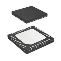
Manufacturer Part Number
R5F213J6CNNP#U0
Description
MCU 1KB FLASH 32K ROM 36-QFN
Manufacturer
Renesas Electronics America
Series
R8C/3x/3JCr
Datasheet
1.R5F213J6CNNPU0.pdf
(750 pages)
Specifications of R5F213J6CNNP#U0
Core Processor
R8C
Core Size
16/32-Bit
Speed
20MHz
Connectivity
I²C, LIN, SIO, SSU, UART/USART
Peripherals
POR, PWM, Voltage Detect, WDT
Number Of I /o
31
Program Memory Size
32KB (32K x 8)
Program Memory Type
FLASH
Ram Size
2.5K x 8
Voltage - Supply (vcc/vdd)
1.8 V ~ 5.5 V
Data Converters
A/D 10x10b, D/A 2x8b
Oscillator Type
Internal
Operating Temperature
-20°C ~ 85°C
Package / Case
36-WQFN Exposed Pad, 36-HWQFN
Lead Free Status / RoHS Status
Lead free / RoHS Compliant
Eeprom Size
-
Available stocks
Company
Part Number
Manufacturer
Quantity
Price


R8C/3JC Group
REJ09B0602-0100 Rev.1.00
May 12, 2010
20.3.11 Timer RD Status Register i (TRDSRi) (i = 0 or 1) in Input Capture Function
Notes:
1. Nothing is assigned to b5 in the TRDSR0 register. When writing to b5, write 0. When reading, the content is 1.
2. The writing results are as follows:
3. Edge selected by bits IOj1 to IOj0 (j = A or B) in the TRDIORAi register.
4. Edge selected by bits IOk1 to IOk0 (k = C or D) in the TRDIORCi register.
After Reset
After Reset
Bit
b0
b1
b2
b3
b4
b5
b6
b7
Address 0143h (TRDSR0), 0153h (TRDSR1)
• This bit is set to 0 when the read result is 1 and 0 is written to the same bit.
• This bit remains unchanged even if the read result is 0 and 0 is written to the same bit. (This bit remains 1 even
• This bit remains unchanged if 1 is written to it.
Including when the BFki bit in the TRDMR register is set to 1 (TRDGRki is used as the buffer register).
Symbol
if it is set to 1 from 0 after reading, and writing 0.)
Symbol
Bit
IMFB
IMFC
IMFD
IMFA
OVF
UDF
—
—
b7
—
1
1
Input capture / compare match flag A [Source for setting this bit to 0]
Input capture / compare match flag B [Source for setting this bit to 0]
Input capture / compare match flag C [Source for setting this bit to 0]
Input capture / compare match flag D [Source for setting this bit to 0]
Overflow flag
Underflow flag
Nothing is assigned. If necessary, set to 0. When read, the content is 1.
b6
—
1
1
Bit Name
(1)
UDF
b5
1
0
OVF
b4
0
0
Write 0 after read
[Source for setting this bit to 1].
TRDSR0 register:
TRDSR1 register:
Write 0 after read
[Source for setting this bit to 1]
Input edge of TRDIOBi pin
Write 0 after read
[Source for setting this bit to 1]
Input edge of TRDIOCi pin
Write 0 after read
[Source for setting this bit to 1]
Input edge of TRDIODi pin
[Source for setting this bit to 0]
Write 0 after read
[Source for setting this bit to 1]
When the TRDi register overflows.
This bit is disabled in the input capture function.
fOCO128 signal edge when the IOA3 bit in the
TRDIORA0 register is set to 0 (fOCO128 signal).
TRDIOA0 pin input edge when the IOA3 bit in the
TRDIORA0 register is set to 1 (TRDIOA0 input)
Input edge of TRDIOA1 pin
IMFD
b3
0
0
IMFC
b2
0
0
(2)
(2)
(2)
(2)
(2)
.
.
.
.
.
Function
IMFB
b1
0
0
(3)
(4)
(4)
(3)
.
.
.
.
IMFA
b0
0
0
TRDSR0 register
TRDSR1 register
Page 312 of 715
20. Timer RD
(3)
.
R/W
R/W
R/W
R/W
R/W
R/W
R/W
—
Related parts for R5F213J6CNNP#U0
Image
Part Number
Description
Manufacturer
Datasheet
Request
R

Part Number:
Description:
KIT STARTER FOR M16C/29
Manufacturer:
Renesas Electronics America
Datasheet:

Part Number:
Description:
KIT STARTER FOR R8C/2D
Manufacturer:
Renesas Electronics America
Datasheet:

Part Number:
Description:
R0K33062P STARTER KIT
Manufacturer:
Renesas Electronics America
Datasheet:

Part Number:
Description:
KIT STARTER FOR R8C/23 E8A
Manufacturer:
Renesas Electronics America
Datasheet:

Part Number:
Description:
KIT STARTER FOR R8C/25
Manufacturer:
Renesas Electronics America
Datasheet:

Part Number:
Description:
KIT STARTER H8S2456 SHARPE DSPLY
Manufacturer:
Renesas Electronics America
Datasheet:

Part Number:
Description:
KIT STARTER FOR R8C38C
Manufacturer:
Renesas Electronics America
Datasheet:

Part Number:
Description:
KIT STARTER FOR R8C35C
Manufacturer:
Renesas Electronics America
Datasheet:

Part Number:
Description:
KIT STARTER FOR R8CL3AC+LCD APPS
Manufacturer:
Renesas Electronics America
Datasheet:
Part Number:
Description:
KIT STARTER FOR RX610
Manufacturer:
Renesas Electronics America
Datasheet:

Part Number:
Description:
KIT STARTER FOR R32C/118
Manufacturer:
Renesas Electronics America
Datasheet:

Part Number:
Description:
KIT DEV RSK-R8C/26-29
Manufacturer:
Renesas Electronics America
Datasheet:

Part Number:
Description:
KIT STARTER FOR SH7124
Manufacturer:
Renesas Electronics America
Datasheet:

Part Number:
Description:
KIT STARTER FOR H8SX/1622
Manufacturer:
Renesas Electronics America
Datasheet:

Part Number:
Description:
KIT DEV FOR SH7203
Manufacturer:
Renesas Electronics America
Datasheet: