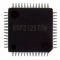
R5F21257SNFP#U0 Renesas Electronics America, R5F21257SNFP#U0 Datasheet - Page 346

R5F21257SNFP#U0
Manufacturer Part Number
R5F21257SNFP#U0
Description
IC R8C/25 MCU FLASH 52LQFP
Manufacturer
Renesas Electronics America
Series
R8C/2x/25r
Specifications of R5F21257SNFP#U0
Core Processor
R8C
Core Size
16/32-Bit
Speed
20MHz
Connectivity
I²C, LIN, SIO, SSU, UART/USART
Peripherals
POR, Voltage Detect, WDT
Number Of I /o
41
Program Memory Size
48KB (48K x 8)
Program Memory Type
FLASH
Ram Size
2.5K x 8
Voltage - Supply (vcc/vdd)
2.2 V ~ 5.5 V
Data Converters
A/D 12x10b
Oscillator Type
Internal
Operating Temperature
-20°C ~ 85°C
Package / Case
52-LQFP
For Use With
R0K521256S000BE - KIT EVAL STARTER FOR R8C/25
Lead Free Status / RoHS Status
Lead free / RoHS Compliant
Eeprom Size
-
Available stocks
Company
Part Number
Manufacturer
Quantity
Price
- Current page: 346 of 527
- Download datasheet (6Mb)
R8C/24 Group, R8C/25 Group
Rev.3.00
REJ09B0244-0300
16.2.6
16.2.6.1
In 4-wire bus communication mode, a 4-wire bus consisting of a clock line, a data input line, a data output line,
and a chip select line is used for communication. This mode includes bidirectional mode in which the data input
line and data output line function as a single pin.
The data input line and output line change according to the settings of the MSS bit in the SSCRH register and
the BIDE bit in the SSMR2 register. For details, refer to 16.2.2.1 Association between Data I/O Pins and SS
Shift Register. In this mode, clock polarity, phase, and data settings are performed by bits CPOS and CPHS in
the SSMR register. For details, refer to 16.2.1.1 Association between Transfer Clock Polarity, Phase, and
Data.
When this MCU is set as the master device, the chip select line controls output. When clock synchronous serial
I/O with chip select is set as a slave device, the chip select line controls input. When it is set as the master
device, the chip select line controls output of the SCS pin or controls output of a general port according to the
setting of the CSS1 bit in the SSMR2 register. When the MCU is set as a slave device, the chip select line sets
the SCS pin as an input pin by setting bits CSS1 and CSS0 in the SSMR2 register to 01b.
In 4-wire bus communication mode, the MLS bit in the SSMR register is set to 0 and communication is
performed MSB-first.
Figure 16.18 shows Initialization in 4-Wire Bus Communication Mode. Before the data transit/receive
operation, set the TE bit in the SSER register to 0 (transmit disabled), the RE bit in the SSER register to 0
(receive disabled), and initialize the clock synchronous serial I/O with chip select.
To change the communication mode or format, set the TE bit to 0 and the RE bit to 0 before making the change.
Setting the RE bit to 0 does not change the settings of flags RDRF and ORER or the contents of the SSRDR
register.
Feb 29, 2008
Operation in 4-Wire Bus Communication Mode
Initialization in 4-Wire Bus Communication Mode
Page 327 of 485
16. Clock Synchronous Serial Interface
Related parts for R5F21257SNFP#U0
Image
Part Number
Description
Manufacturer
Datasheet
Request
R

Part Number:
Description:
KIT STARTER FOR M16C/29
Manufacturer:
Renesas Electronics America
Datasheet:

Part Number:
Description:
KIT STARTER FOR R8C/2D
Manufacturer:
Renesas Electronics America
Datasheet:

Part Number:
Description:
R0K33062P STARTER KIT
Manufacturer:
Renesas Electronics America
Datasheet:

Part Number:
Description:
KIT STARTER FOR R8C/23 E8A
Manufacturer:
Renesas Electronics America
Datasheet:

Part Number:
Description:
KIT STARTER FOR R8C/25
Manufacturer:
Renesas Electronics America
Datasheet:

Part Number:
Description:
KIT STARTER H8S2456 SHARPE DSPLY
Manufacturer:
Renesas Electronics America
Datasheet:

Part Number:
Description:
KIT STARTER FOR R8C38C
Manufacturer:
Renesas Electronics America
Datasheet:

Part Number:
Description:
KIT STARTER FOR R8C35C
Manufacturer:
Renesas Electronics America
Datasheet:

Part Number:
Description:
KIT STARTER FOR R8CL3AC+LCD APPS
Manufacturer:
Renesas Electronics America
Datasheet:

Part Number:
Description:
KIT STARTER FOR RX610
Manufacturer:
Renesas Electronics America
Datasheet:

Part Number:
Description:
KIT STARTER FOR R32C/118
Manufacturer:
Renesas Electronics America
Datasheet:

Part Number:
Description:
KIT DEV RSK-R8C/26-29
Manufacturer:
Renesas Electronics America
Datasheet:

Part Number:
Description:
KIT STARTER FOR SH7124
Manufacturer:
Renesas Electronics America
Datasheet:

Part Number:
Description:
KIT STARTER FOR H8SX/1622
Manufacturer:
Renesas Electronics America
Datasheet:

Part Number:
Description:
KIT DEV FOR SH7203
Manufacturer:
Renesas Electronics America
Datasheet:


