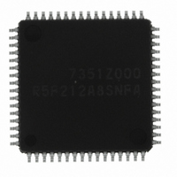
R5F212A8SNFA#U0 Renesas Electronics America, R5F212A8SNFA#U0 Datasheet - Page 235

R5F212A8SNFA#U0
Manufacturer Part Number
R5F212A8SNFA#U0
Description
IC R8C/2A MCU FLASH 64K 64-LQFP
Manufacturer
Renesas Electronics America
Series
R8C/2x/2Ar
Specifications of R5F212A8SNFA#U0
Core Processor
R8C
Core Size
16/32-Bit
Speed
20MHz
Connectivity
I²C, LIN, SIO, SSU, UART/USART
Peripherals
POR, PWM, Voltage Detect, WDT
Number Of I /o
55
Program Memory Size
64KB (64K x 8)
Program Memory Type
FLASH
Ram Size
3K x 8
Voltage - Supply (vcc/vdd)
2.2 V ~ 5.5 V
Data Converters
A/D 12x10b; D/A 2x8b
Oscillator Type
Internal
Operating Temperature
-20°C ~ 85°C
Package / Case
64-LQFP
For Use With
R0K5212D8S001BE - KIT STARTER FOR R8C/2DR0K5212D8S000BE - KIT DEV FOR R8C/2D
Lead Free Status / RoHS Status
Lead free / RoHS Compliant
Eeprom Size
-
Available stocks
Company
Part Number
Manufacturer
Quantity
Price
Part Number:
R5F212A8SNFA#U0R5F212A8SNFA#V2
Manufacturer:
Renesas Electronics America
Quantity:
10 000
- Current page: 235 of 611
- Download datasheet (7Mb)
R8C/2A Group, R8C/2B Group
Rev.2.00
REJ09B0324-0200
14.3.4
Table 14.17
j = A, B, C, or D
Count source
Count operation
Count period
Count start condition
Count stop condition
Interrupt request generation
timing
TRCIOA, TRCIOB, TRCIOC,
and TRCIOD pin functions
INT0 pin function
Read from timer
Write to timer
Select functions
This function measures the width or period of an external signal. An external signal input to the TRCIOj (j = A,
B, C, or D) pin acts as a trigger for transferring the contents of the TRC register (counter) to the TRCGRj
register (input capture). The input capture function, or any other mode or function, can be selected for each
individual pin.
The TRCGRA register can also select fOCO128 signal as input-capture trigger input.
Table 14.17 lists the Specifications of Input Capture Function, Figure 14.43 shows a Block Diagram of Input
Capture Function, Figures 14.44 and 14.45 show registers associated with the input capture function, Table
14.18 lists the Functions of TRCGRj Register when Using Input Capture Function, and Figure 14.46 shows an
Operating Example of Input Capture Function.
Nov 26, 2007
Timer Mode (Input Capture Function)
Item
Specifications of Input Capture Function
Page 213 of 580
f1, f2, f4, f8, f32, fOCO40M, or external signal (rising edge) input to
TRCCLK pin
Increment
1/fk × 65,536 fk: Count source frequency
1 (count starts) is written to the TSTART bit in the TRCMR register.
0 (count stops) is written to the TSTART bit in the TRCMR register.
The TRC register retains a value before count stops.
• Input capture (valid edge of TRCIOj input or fOCO128 signal edge)
• The TRC register overflows.
Programmable I/O port or input capture input (selectable individually by
pin)
Programmable I/O port or INT0 interrupt input
The count value can be read by reading TRC register.
The TRC register can be written to.
• Input capture input pin select
• Input capture input valid edge selected
• Buffer operation (Refer to 14.3.3.2 Buffer Operation.)
• Digital filter (Refer to 14.3.3.3 Digital Filter.)
• Input-capture trigger selected
One or more of pins TRCIOA, TRCIOB, TRCIOC, and TRCIOD
Rising edge, falling edge, or both rising and falling edges
fOCO128 can be selected for input-capture trigger input of the
TRCGRA register.
Specification
14. Timers
Related parts for R5F212A8SNFA#U0
Image
Part Number
Description
Manufacturer
Datasheet
Request
R

Part Number:
Description:
KIT STARTER FOR M16C/29
Manufacturer:
Renesas Electronics America
Datasheet:

Part Number:
Description:
KIT STARTER FOR R8C/2D
Manufacturer:
Renesas Electronics America
Datasheet:

Part Number:
Description:
R0K33062P STARTER KIT
Manufacturer:
Renesas Electronics America
Datasheet:

Part Number:
Description:
KIT STARTER FOR R8C/23 E8A
Manufacturer:
Renesas Electronics America
Datasheet:

Part Number:
Description:
KIT STARTER FOR R8C/25
Manufacturer:
Renesas Electronics America
Datasheet:

Part Number:
Description:
KIT STARTER H8S2456 SHARPE DSPLY
Manufacturer:
Renesas Electronics America
Datasheet:

Part Number:
Description:
KIT STARTER FOR R8C38C
Manufacturer:
Renesas Electronics America
Datasheet:

Part Number:
Description:
KIT STARTER FOR R8C35C
Manufacturer:
Renesas Electronics America
Datasheet:

Part Number:
Description:
KIT STARTER FOR R8CL3AC+LCD APPS
Manufacturer:
Renesas Electronics America
Datasheet:

Part Number:
Description:
KIT STARTER FOR RX610
Manufacturer:
Renesas Electronics America
Datasheet:

Part Number:
Description:
KIT STARTER FOR R32C/118
Manufacturer:
Renesas Electronics America
Datasheet:

Part Number:
Description:
KIT DEV RSK-R8C/26-29
Manufacturer:
Renesas Electronics America
Datasheet:

Part Number:
Description:
KIT STARTER FOR SH7124
Manufacturer:
Renesas Electronics America
Datasheet:

Part Number:
Description:
KIT STARTER FOR H8SX/1622
Manufacturer:
Renesas Electronics America
Datasheet:

Part Number:
Description:
KIT DEV FOR SH7203
Manufacturer:
Renesas Electronics America
Datasheet:


