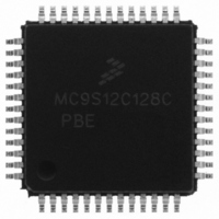
MC9S12C128CPBE Freescale Semiconductor, MC9S12C128CPBE Datasheet - Page 241

MC9S12C128CPBE
Manufacturer Part Number
MC9S12C128CPBE
Description
IC MCU 128K FLASH 25MHZ 52-LQFP
Manufacturer
Freescale Semiconductor
Series
HCS12r
Specifications of MC9S12C128CPBE
Core Processor
HCS12
Core Size
16-Bit
Speed
25MHz
Connectivity
CAN, EBI/EMI, SCI, SPI
Peripherals
POR, PWM, WDT
Number Of I /o
35
Program Memory Size
128KB (128K x 8)
Program Memory Type
FLASH
Ram Size
4K x 8
Voltage - Supply (vcc/vdd)
2.35 V ~ 5.5 V
Data Converters
A/D 8x10b
Oscillator Type
Internal
Operating Temperature
-40°C ~ 85°C
Package / Case
52-LQFP
Lead Free Status / RoHS Status
Lead free / RoHS Compliant
Eeprom Size
-
Available stocks
Company
Part Number
Manufacturer
Quantity
Price
Company:
Part Number:
MC9S12C128CPBE
Manufacturer:
Freescale Semiconductor
Quantity:
10 000
Company:
Part Number:
MC9S12C128CPBER
Manufacturer:
Freescale Semiconductor
Quantity:
10 000
- Current page: 241 of 690
- Download datasheet (4Mb)
8.3.2.10
This read-only register contains the Conversion Complete Flags.
Read: Anytime
Write: Anytime, no effect
Freescale Semiconductor
Module Base + 0x000B
CCF[7:0]
Reset
Field
7–0
W
R
CCF7
Conversion Complete Flag x (x = 7, 6, 5, 4, 3, 2, 1, 0) — A conversion complete flag is set at the end of each
conversion in a conversion sequence. The flags are associated with the conversion position in a sequence (and
also the result register number). Therefore, CCF0 is set when the first conversion in a sequence is complete and
the result is available in result register ATDDR0; CCF1 is set when the second conversion in a sequence is
complete and the result is available in ATDDR1, and so forth. A flag CCFx (x = 7, 6, 5, 4, 3, 2, 1, 0) is cleared
when one of the following occurs:
0 Conversion number x not completed
1 Conversion number x has completed, result ready in ATDDRx
ATD Status Register 1 (ATDSTAT1)
0
7
A) Write to ATDCTL5 (a new conversion sequence is started)
B) If AFFC = 0 and read of ATDSTAT1 followed by read of result register ATDDRx
C) If AFFC = 1 and read of result register ATDDRx
= Unimplemented or Reserved
CCF6
0
6
Figure 8-12. ATD Status Register 1 (ATDSTAT1)
Table 8-16. ATDSTAT1 Field Descriptions
CCF5
MC9S12C-Family / MC9S12GC-Family
0
5
CCF4
Rev 01.24
0
4
Chapter 8 Analog-to-Digital Converter (ATD10B8C) Block Description
Description
CCF3
0
3
CCF2
0
2
CCF1
0
1
CCF0
0
0
241
Related parts for MC9S12C128CPBE
Image
Part Number
Description
Manufacturer
Datasheet
Request
R
Part Number:
Description:
Manufacturer:
Freescale Semiconductor, Inc
Datasheet:
Part Number:
Description:
Manufacturer:
Freescale Semiconductor, Inc
Datasheet:
Part Number:
Description:
Manufacturer:
Freescale Semiconductor, Inc
Datasheet:
Part Number:
Description:
Manufacturer:
Freescale Semiconductor, Inc
Datasheet:
Part Number:
Description:
Manufacturer:
Freescale Semiconductor, Inc
Datasheet:
Part Number:
Description:
Manufacturer:
Freescale Semiconductor, Inc
Datasheet:
Part Number:
Description:
Manufacturer:
Freescale Semiconductor, Inc
Datasheet:
Part Number:
Description:
Manufacturer:
Freescale Semiconductor, Inc
Datasheet:
Part Number:
Description:
Manufacturer:
Freescale Semiconductor, Inc
Datasheet:
Part Number:
Description:
Manufacturer:
Freescale Semiconductor, Inc
Datasheet:
Part Number:
Description:
Manufacturer:
Freescale Semiconductor, Inc
Datasheet:
Part Number:
Description:
Manufacturer:
Freescale Semiconductor, Inc
Datasheet:
Part Number:
Description:
Manufacturer:
Freescale Semiconductor, Inc
Datasheet:
Part Number:
Description:
Manufacturer:
Freescale Semiconductor, Inc
Datasheet:
Part Number:
Description:
Manufacturer:
Freescale Semiconductor, Inc
Datasheet:


