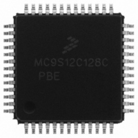
MC9S12C128CPBE Freescale Semiconductor, MC9S12C128CPBE Datasheet - Page 56

MC9S12C128CPBE
Manufacturer Part Number
MC9S12C128CPBE
Description
IC MCU 128K FLASH 25MHZ 52-LQFP
Manufacturer
Freescale Semiconductor
Series
HCS12r
Specifications of MC9S12C128CPBE
Core Processor
HCS12
Core Size
16-Bit
Speed
25MHz
Connectivity
CAN, EBI/EMI, SCI, SPI
Peripherals
POR, PWM, WDT
Number Of I /o
35
Program Memory Size
128KB (128K x 8)
Program Memory Type
FLASH
Ram Size
4K x 8
Voltage - Supply (vcc/vdd)
2.35 V ~ 5.5 V
Data Converters
A/D 8x10b
Oscillator Type
Internal
Operating Temperature
-40°C ~ 85°C
Package / Case
52-LQFP
Lead Free Status / RoHS Status
Lead free / RoHS Compliant
Eeprom Size
-
Available stocks
Company
Part Number
Manufacturer
Quantity
Price
Company:
Part Number:
MC9S12C128CPBE
Manufacturer:
Freescale Semiconductor
Quantity:
10 000
Company:
Part Number:
MC9S12C128CPBER
Manufacturer:
Freescale Semiconductor
Quantity:
10 000
- Current page: 56 of 690
- Download datasheet (4Mb)
Chapter 1 MC9S12C and MC9S12GC Device Overview (MC9S12C128)
1.3.5.4
V
to digital converter.
1.3.5.5
V
1.3.5.6
Provides operating voltage and ground for the oscillator and the phased-locked loop. This allows the
supply voltage to the oscillator and PLL to be bypassed independently. This 2.5V voltage is generated by
the internal voltage regulator.
56
Mnemonic
V
DDA
RH
V
DD1, VDD2
SS1, VSS2
V
V
V
V
V
V
V
V
V
DDPLL
SSPLL
V
and V
DDR
SSR
DDX
SSX
DDA
SSA
RH
RL
, V
SSA
RL
are the power supply and ground input pins for the voltage regulator reference and the analog
V
V
V
Voltage (V)
are the reference voltage input pins for the analog to digital converter.
Nominal
All V
signal transitions place high, short-duration current demands on the power
supply, use bypass capacitors with high-frequency characteristics and place
them as close to the MCU as possible. Bypass requirements depend on
MCU pin load.
DDA
RH
DDPLL
2.5
5.0
5.0
5.0
5.0
2.5
0
0
0
0
0
0
, V
, V
SS
RL
, V
SSA
pins must be connected together in the application. Because fast
Internal power and ground generated by internal regulator. These also allow an external source
to supply the core V
In the 48 and 52 LQFP packages V
External power and ground, supply to internal voltage regulator.
External power and ground, supply to pin drivers.
Operating voltage and ground for the analog-to-digital converters and the reference for the
internal voltage regulator, allows the supply voltage to the A/D to be bypassed independently.
Reference voltage low for the ATD converter.
In the 48 and 52 LQFP packages V
Provides operating voltage and ground for the phased-locked loop. This allows the supply voltage
to the PLL to be bypassed independently. Internal power and ground generated by internal
regulator.
— ATD Reference Voltage Input Pins
SSPLL
Table 1-6. Power and Ground Connection Summary
— Power Supply Pins for ATD and VREG
— Power Supply Pins for PLL
MC9S12C-Family / MC9S12GC-Family
DD
/V
SS
voltages and bypass the internal voltage regulator.
Rev 01.24
NOTE
DD2
RL
is bonded to V
and V
Description
SS2
are not available.
SSA
.
Freescale Semiconductor
Related parts for MC9S12C128CPBE
Image
Part Number
Description
Manufacturer
Datasheet
Request
R
Part Number:
Description:
Manufacturer:
Freescale Semiconductor, Inc
Datasheet:
Part Number:
Description:
Manufacturer:
Freescale Semiconductor, Inc
Datasheet:
Part Number:
Description:
Manufacturer:
Freescale Semiconductor, Inc
Datasheet:
Part Number:
Description:
Manufacturer:
Freescale Semiconductor, Inc
Datasheet:
Part Number:
Description:
Manufacturer:
Freescale Semiconductor, Inc
Datasheet:
Part Number:
Description:
Manufacturer:
Freescale Semiconductor, Inc
Datasheet:
Part Number:
Description:
Manufacturer:
Freescale Semiconductor, Inc
Datasheet:
Part Number:
Description:
Manufacturer:
Freescale Semiconductor, Inc
Datasheet:
Part Number:
Description:
Manufacturer:
Freescale Semiconductor, Inc
Datasheet:
Part Number:
Description:
Manufacturer:
Freescale Semiconductor, Inc
Datasheet:
Part Number:
Description:
Manufacturer:
Freescale Semiconductor, Inc
Datasheet:
Part Number:
Description:
Manufacturer:
Freescale Semiconductor, Inc
Datasheet:
Part Number:
Description:
Manufacturer:
Freescale Semiconductor, Inc
Datasheet:
Part Number:
Description:
Manufacturer:
Freescale Semiconductor, Inc
Datasheet:
Part Number:
Description:
Manufacturer:
Freescale Semiconductor, Inc
Datasheet:


