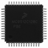
MC9S12C128CPBE Freescale Semiconductor, MC9S12C128CPBE Datasheet - Page 669

MC9S12C128CPBE
Manufacturer Part Number
MC9S12C128CPBE
Description
IC MCU 128K FLASH 25MHZ 52-LQFP
Manufacturer
Freescale Semiconductor
Series
HCS12r
Specifications of MC9S12C128CPBE
Core Processor
HCS12
Core Size
16-Bit
Speed
25MHz
Connectivity
CAN, EBI/EMI, SCI, SPI
Peripherals
POR, PWM, WDT
Number Of I /o
35
Program Memory Size
128KB (128K x 8)
Program Memory Type
FLASH
Ram Size
4K x 8
Voltage - Supply (vcc/vdd)
2.35 V ~ 5.5 V
Data Converters
A/D 8x10b
Oscillator Type
Internal
Operating Temperature
-40°C ~ 85°C
Package / Case
52-LQFP
Lead Free Status / RoHS Status
Lead free / RoHS Compliant
Eeprom Size
-
Available stocks
Company
Part Number
Manufacturer
Quantity
Price
Company:
Part Number:
MC9S12C128CPBE
Manufacturer:
Freescale Semiconductor
Quantity:
10 000
Company:
Part Number:
MC9S12C128CPBER
Manufacturer:
Freescale Semiconductor
Quantity:
10 000
- Current page: 669 of 690
- Download datasheet (4Mb)
1. % deviation from target frequency
2. f
A.5
A.5.1
The time base for all NVM program or erase operations is derived from the oscillator. A minimum
oscillator frequency f
do not have any means to monitor the frequency and will not prevent program or erase operation at
frequencies above or below the specified minimum. Attempting to program or erase the NVM modules at
a lower frequency a full program or erase transition is not assured.
The Flash program and erase operations are timed using a clock derived from the oscillator using the
FCLKDIV and ECLKDIV registers respectively. The frequency of this clock must be set within the limits
specified as f
The minimum program and erase times shown in
maximum f
Freescale Semiconductor
Conditions are shown in
Num C
10
11
12
13
14
15
1
2
3
4
5
6
7
8
9
OSC
= 4MHz, f
D VCO locking range
D
D Lock Detection
D Un-Lock Detection
D
C PLLON Total Stabilization delay (Auto Mode)
D PLLON
D PLLON Tracking mode stabilization delay
D Fitting parameter VCO loop gain
D Fitting parameter VCO loop frequency
D Charge pump current acquisition mode
D Charge pump current tracking mode
C Jitter fit parameter 1
C Jitter fit parameter 2
P Self Clock Mode frequency
Lock Detector transition from Acquisition to Tracking
mode
Lock Detector transition from Tracking to Acquisition
mode
NVM, Flash, and EEPROM
bus
NVM Timing
NVMOP
BUS
. The maximum times are calculated for minimum f
Acquisition
= 25MHz equivalent f
.
Table A-4
NVMOSC
mode stabilization delay
2
2
Rating
unless otherwise noted
is required for performing program or erase operations. The NVM modules
VCO
MC9S12C-Family / MC9S12GC-Family
Table A-17. PLL Characteristics
= 50MHz: REFDV = #$03, SYNR = #$018, Cs = 4.7nF, Cp = 470pF, Rs = 10K
2
2
(2)
Rev 01.24
Table A-18
Symbol
|∆
f
|∆
|∆
| i
| i
f
|∆
t
t
SCM
VCO
stab
Lock|
acq
K
t
f
ch
ch
j
j
unt|
unl|
al
trk|
1
2
1
1
|
|
are calculated for maximum f
NVMOP
Min
0.5
—
—
—
—
—
—
—
—
—
1
8
3
0
6
and a f
Appendix A Electrical Characteristics
-100
38.5
Typ
0.5
0.3
0.2
3.5
—
—
—
—
—
—
60
—
—
bus
of 2MHz.
Max
0.13
5.5
1.5
2.5
1.1
50
—
—
—
—
—
—
—
NVMOP
4
8
MHz/V
and
MHz
MHz
MHz
Unit
%
%
%
%
ms
ms
ms
µA
µA
%
%
(1)
1
1
1
669
Ω
.
Related parts for MC9S12C128CPBE
Image
Part Number
Description
Manufacturer
Datasheet
Request
R
Part Number:
Description:
Manufacturer:
Freescale Semiconductor, Inc
Datasheet:
Part Number:
Description:
Manufacturer:
Freescale Semiconductor, Inc
Datasheet:
Part Number:
Description:
Manufacturer:
Freescale Semiconductor, Inc
Datasheet:
Part Number:
Description:
Manufacturer:
Freescale Semiconductor, Inc
Datasheet:
Part Number:
Description:
Manufacturer:
Freescale Semiconductor, Inc
Datasheet:
Part Number:
Description:
Manufacturer:
Freescale Semiconductor, Inc
Datasheet:
Part Number:
Description:
Manufacturer:
Freescale Semiconductor, Inc
Datasheet:
Part Number:
Description:
Manufacturer:
Freescale Semiconductor, Inc
Datasheet:
Part Number:
Description:
Manufacturer:
Freescale Semiconductor, Inc
Datasheet:
Part Number:
Description:
Manufacturer:
Freescale Semiconductor, Inc
Datasheet:
Part Number:
Description:
Manufacturer:
Freescale Semiconductor, Inc
Datasheet:
Part Number:
Description:
Manufacturer:
Freescale Semiconductor, Inc
Datasheet:
Part Number:
Description:
Manufacturer:
Freescale Semiconductor, Inc
Datasheet:
Part Number:
Description:
Manufacturer:
Freescale Semiconductor, Inc
Datasheet:
Part Number:
Description:
Manufacturer:
Freescale Semiconductor, Inc
Datasheet:


