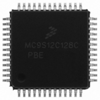
MC9S12C128CPBE Freescale Semiconductor, MC9S12C128CPBE Datasheet - Page 409

MC9S12C128CPBE
Manufacturer Part Number
MC9S12C128CPBE
Description
IC MCU 128K FLASH 25MHZ 52-LQFP
Manufacturer
Freescale Semiconductor
Series
HCS12r
Specifications of MC9S12C128CPBE
Core Processor
HCS12
Core Size
16-Bit
Speed
25MHz
Connectivity
CAN, EBI/EMI, SCI, SPI
Peripherals
POR, PWM, WDT
Number Of I /o
35
Program Memory Size
128KB (128K x 8)
Program Memory Type
FLASH
Ram Size
4K x 8
Voltage - Supply (vcc/vdd)
2.35 V ~ 5.5 V
Data Converters
A/D 8x10b
Oscillator Type
Internal
Operating Temperature
-40°C ~ 85°C
Package / Case
52-LQFP
Lead Free Status / RoHS Status
Lead free / RoHS Compliant
Eeprom Size
-
Available stocks
Company
Part Number
Manufacturer
Quantity
Price
Company:
Part Number:
MC9S12C128CPBE
Manufacturer:
Freescale Semiconductor
Quantity:
10 000
Company:
Part Number:
MC9S12C128CPBER
Manufacturer:
Freescale Semiconductor
Quantity:
10 000
- Current page: 409 of 690
- Download datasheet (4Mb)
13.4.5
Normally, the SCI uses two pins for transmitting and receiving. In single-wire operation, the RXD pin is
disconnected from the SCI. The SCI uses the TXD pin for both receiving and transmitting.
Enable single-wire operation by setting the LOOPS bit and the receiver source bit, RSRC, in SCI control
register 1 (SCICR1). Setting the LOOPS bit disables the path from the Rx Input signal to the receiver.
Setting the RSRC bit connects the receiver input to the output of the TXD pin driver. Both the transmitter
and receiver must be enabled (TE = 1 and RE = 1).The TXDIR bit (SCISR2[1]) determines whether the
TXD pin is going to be used as an input (TXDIR = 0) or an output (TXDIR = 1) in this mode of operation.
13.4.6
In loop operation the transmitter output goes to the receiver input. The Rx Input signal is disconnected
from the SCI
Enable loop operation by setting the LOOPS bit and clearing the RSRC bit in SCI control register 1
(SCICR1). Setting the LOOPS bit disables the path from the Rx Input signal to the receiver. Clearing the
RSRC bit connects the transmitter output to the receiver input. Both the transmitter and receiver must be
enabled (TE = 1 and RE = 1).
13.5
13.5.1
The reset state of each individual bit is listed in
the registers and their bit fields. All special functions or modes which are initialized during or just
following reset are described within this section.
Freescale Semiconductor
.
Initialization Information
Single-Wire Operation
Loop Operation
Reset Initialization
Figure 13-22. Single-Wire Operation (LOOPS = 1, RSRC = 1)
Figure 13-23. Loop Operation (LOOPS = 1, RSRC = 0)
TRANSMITTER
TRANSMITTER
RECEIVER
RECEIVER
MC9S12C-Family / MC9S12GC-Family
Chapter 13 Serial Communications Interface (S12SCIV2) Block Description
Section 13.3, “Memory Map and Registers”
Rev 01.24
Tx OUTPUT SIGNAL
Tx OUTPUT SIGNAL
Tx INPUT SIGNAL
RXD
RXD
which details
409
Related parts for MC9S12C128CPBE
Image
Part Number
Description
Manufacturer
Datasheet
Request
R
Part Number:
Description:
Manufacturer:
Freescale Semiconductor, Inc
Datasheet:
Part Number:
Description:
Manufacturer:
Freescale Semiconductor, Inc
Datasheet:
Part Number:
Description:
Manufacturer:
Freescale Semiconductor, Inc
Datasheet:
Part Number:
Description:
Manufacturer:
Freescale Semiconductor, Inc
Datasheet:
Part Number:
Description:
Manufacturer:
Freescale Semiconductor, Inc
Datasheet:
Part Number:
Description:
Manufacturer:
Freescale Semiconductor, Inc
Datasheet:
Part Number:
Description:
Manufacturer:
Freescale Semiconductor, Inc
Datasheet:
Part Number:
Description:
Manufacturer:
Freescale Semiconductor, Inc
Datasheet:
Part Number:
Description:
Manufacturer:
Freescale Semiconductor, Inc
Datasheet:
Part Number:
Description:
Manufacturer:
Freescale Semiconductor, Inc
Datasheet:
Part Number:
Description:
Manufacturer:
Freescale Semiconductor, Inc
Datasheet:
Part Number:
Description:
Manufacturer:
Freescale Semiconductor, Inc
Datasheet:
Part Number:
Description:
Manufacturer:
Freescale Semiconductor, Inc
Datasheet:
Part Number:
Description:
Manufacturer:
Freescale Semiconductor, Inc
Datasheet:
Part Number:
Description:
Manufacturer:
Freescale Semiconductor, Inc
Datasheet:


