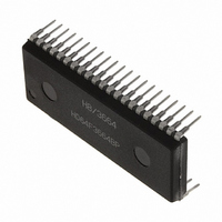
M38513E4FP#U0 Renesas Electronics America, M38513E4FP#U0 Datasheet - Page 44

M38513E4FP#U0
Manufacturer Part Number
M38513E4FP#U0
Description
IC 740 MCU ROM 16K 42SSOP
Manufacturer
Renesas Electronics America
Series
740/38000r
Specifications of M38513E4FP#U0
Core Processor
740
Core Size
8-Bit
Speed
8MHz
Connectivity
SIO, UART/USART
Peripherals
PWM, WDT
Number Of I /o
34
Program Memory Size
16KB (16K x 8)
Program Memory Type
OTP
Ram Size
512 x 8
Voltage - Supply (vcc/vdd)
2.7 V ~ 5.5 V
Data Converters
A/D 5x10b
Oscillator Type
External
Operating Temperature
-20°C ~ 85°C
Package / Case
42-SSOP
Package
42SSOP
Family Name
740
Maximum Speed
8 MHz
Operating Supply Voltage
5 V
Data Bus Width
8 Bit
Number Of Programmable I/os
34
Interface Type
I2C-BUS
On-chip Adc
5-chx10-bit
Number Of Timers
4
Lead Free Status / RoHS Status
Contains lead / RoHS non-compliant
Eeprom Size
-
3851 Group
A-D CONVERTER
[A-D Conversion Registers (ADL, ADH)]
0035
The A-D conversion registers are read-only registers that store the
result of an A-D conversion. Do not read these registers during an
A-D conversion.
[A-D Control Register (ADCON)] 0034
The AD control register controls the A-D conversion process. Bits
0 to 2 select a specific analog input pin. Bit 4 indicates the
completion of an A-D conversion. The value of this bit remains at
“0” during an A-D conversion and changes to “1” when an A-D
conversion ends. Writing “0” to this bit starts the A-D conversion.
Comparison Voltage Generator
The comparison voltage generator divides the voltage between
AV
Channel Selector
The channel selector selects one of ports P3
inputs the voltage to the comparator.
Comparator and Control Circuit
The comparator and control circuit compare an analog input volt-
age with the comparison voltage, and the result is stored in the
A-D conversion registers. When an A-D conversion is completed,
the control circuit sets the A-D conversion completion bit and the
A-D interrupt request bit to “1”.
Note that because the comparator consists of a capacitor cou-
pling, set f(X
When the A-D converter is operated at low-speed mode, f(X
and f(X
the A-D converter has a built-in self-oscillation circuit.
Fig. 46 Block diagram of A-D converter
Rev.1.01
SS
and V
16
CIN
, 0036
) do not have the lower limit of frequency, because of
REF
IN
Oct 15, 2003
) to 500 kHz or more during an A-D conversion.
(Built-in 24 KB or more ROM)
into 1024 and outputs the divided voltages.
16
A - D c o n t r o l r e g i s t e r
P 3
P 3
P3
P 3
P 3
( A d d r e s s 0 0 3 4
0
1
2
3
4
/ A N
/ A N
/AN
/ A N
/ A N
0
1
2
3
4
page 42 of 89
1 6
)
0
/AN
Comparator
b 7
3
0
to P3
16
4
/AN
A - D c o n t r o l c i r c u i t
Data bus
4
and
IN
A - D c o n v e r s i o n l o w - o r d e r r e g i s t e r
A-D conversion high-order register
)
R e s i s t o r l a d d e r
V
R E F
Fig. 44 Structure of A-D control register
Fig. 45 Structure of A-D conversion registers
A V
10
N o t e : T h e h i g h - o r d e r 6 b i t s o f a d d r e s s 0 0 3 6
1 0 - b i t r e a d i n g
8 - b i t r e a d i n g ( R e a d o n l y a d d r e s s 0 0 3 5
b7
S S
( R e a d a d d r e s s 0 0 3 6
( A d d r e s s 0 0 3 6
( A d d r e s s 0 0 3 5
( A d d r e s s 0 0 3 5
b 0
a t r e a d i n g .
A - D i n t e r r u p t r e q u e s t
1 6
1 6
1 6
( A d d r e s s 0 0 3 6
( A d d r e s s 0 0 3 5
b 0
)
)
)
A - D c o n t r o l r e g i s t e r
( A D C O N : a d d r e s s 0 0 3 4
Not used (returns “0” when read)
A-D conversion completion bit
b 7
Analog input pin selection bits
Not used (returns “0” when read)
b7
b 7
b 7 b 6 b 5 b 4 b 3 b 2 b 1 b 0
b9 b8 b7 b6 b5 b4 b3 b2
1 6
b 2 b 1 b 0
0 0 0: P3
0 0 1: P3
0 1 0: P3
0 1 1: P3
1 0 0: P3
0: Conversion in progress
1: Conversion completed
b e f o r e 0 0 3 5
1 6
1 6
)
)
0
1
2
3
4
/AN
/AN
/AN
/AN
/AN
1 6
0
1
2
3
4
b e c o m e “ 0 ”
1 6
1 6
)
b 9
1 6
)
)
b 0
b 8
b 0
b0


