M38513E4FP#U0 Renesas Electronics America, M38513E4FP#U0 Datasheet - Page 57
M38513E4FP#U0
Manufacturer Part Number
M38513E4FP#U0
Description
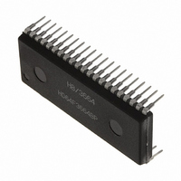
IC 740 MCU ROM 16K 42SSOP
Manufacturer
Renesas Electronics America
Series
740/38000r
Specifications of M38513E4FP#U0
Core Processor
740
Core Size
8-Bit
Speed
8MHz
Connectivity
SIO, UART/USART
Peripherals
PWM, WDT
Number Of I /o
34
Program Memory Size
16KB (16K x 8)
Program Memory Type
OTP
Ram Size
512 x 8
Voltage - Supply (vcc/vdd)
2.7 V ~ 5.5 V
Data Converters
A/D 5x10b
Oscillator Type
External
Operating Temperature
-20°C ~ 85°C
Package / Case
42-SSOP
Package
42SSOP
Family Name
740
Maximum Speed
8 MHz
Operating Supply Voltage
5 V
Data Bus Width
8 Bit
Number Of Programmable I/os
34
Interface Type
I2C-BUS
On-chip Adc
5-chx10-bit
Number Of Timers
4
Lead Free Status / RoHS Status
Contains lead / RoHS non-compliant
Eeprom Size
-


3851 Group
By writing the command code “20
confirmation command code “20
follows, the operation of erase all blocks (erase and erase verify)
starts.
Whether the erase all blocks command is terminated can be con-
firmed by reading the status register or the RY/BY Status Flag of
flash memory control register. When the erase all blocks operation
starts, the read status register mode is entered automatically and
the contents of the status register can be read out at the data bus
(D
time the erase operation starts and is returned to “1” upon comple-
tion of the erase operation. In this case, the read status register
mode remains active until another command is written.
The RY/BY Status Flag is “0” during erase operation and “1” when
the erase operation is completed as is the status register bit 7
(SR7).
After the erase all blocks end, erase results can be checked by
reading bit 5 (SRS) of the status register. For details, refer to the
section where the status register is detailed.
By writing the command code “20
confirmation command code “D0
second bus cycle that follows, the block erase (erase and erase
verify) operation starts for the block address of the flash memory
to be specified.
Whether the block erase operation is completed can be confirmed
by reading the status register or the RY/BY Status Flag of flash
memory control register. At the same time the block erase opera-
tion starts, the read status register mode is automatically entered,
so that the contents of the status register can be read out. The
status register bit 7 (SR7) is set to “0” at the same time the block
erase operation starts and is returned to “1” upon completion of
the block erase operation. In this case, the read status register
mode remains active until the read array command (FF
ten.
The RY/BY Status Flag is “0” during block erase operation and “1”
when the block erase operation is completed as is the status reg-
ister bit 7.
After the block erase ends, erase results can be checked by read-
ing bit 5 (SRS) of the status register. For details, refer to the
section where the status register is detailed.
Rev.1.01
Erase All Blocks Command (20
Block Erase Command (20
0
to D
7
____
____
). The status register bit 7 (SR7) is set to “0” at the same
Oct 15, 2003
(Built-in 24 KB or more ROM)
page 55 of 89
16
/D0
16
16
16
16
16
” in the second bus cycle that
” and the block address in the
” in the first bus cycle and the
16
” in the first bus cycle and the
/20
)
16
____
)
____
16
) is writ-
Fig. 61 Erase flowchart
Write
( R e a d c o m a n d “ F F
E r a s e c o m p l e t e d
S t a t u s r e g i s t e r
RY/BY = 1 ?
S R 5 = 0 ?
W r i t e 2 0
SR7 = 1 ?
B l o c k a d d r e s s
w r i t e )
S t a r t
r e a d
2 0
or
1 6
Y E S
YES
/ D 0
1 6
1 6
1 6
”
N O
N O
2 0
D 0
1 6
1 6
: E r a s e a l l b l o c k s c o m m a n d
: B l o c k e r a s e c o m m a n d
E r a s e e r r o r
Related parts for M38513E4FP#U0
Image
Part Number
Description
Manufacturer
Datasheet
Request
R

Part Number:
Description:
KIT STARTER FOR M16C/29
Manufacturer:
Renesas Electronics America
Datasheet:

Part Number:
Description:
KIT STARTER FOR R8C/2D
Manufacturer:
Renesas Electronics America
Datasheet:

Part Number:
Description:
R0K33062P STARTER KIT
Manufacturer:
Renesas Electronics America
Datasheet:

Part Number:
Description:
KIT STARTER FOR R8C/23 E8A
Manufacturer:
Renesas Electronics America
Datasheet:

Part Number:
Description:
KIT STARTER FOR R8C/25
Manufacturer:
Renesas Electronics America
Datasheet:

Part Number:
Description:
KIT STARTER H8S2456 SHARPE DSPLY
Manufacturer:
Renesas Electronics America
Datasheet:

Part Number:
Description:
KIT STARTER FOR R8C38C
Manufacturer:
Renesas Electronics America
Datasheet:

Part Number:
Description:
KIT STARTER FOR R8C35C
Manufacturer:
Renesas Electronics America
Datasheet:

Part Number:
Description:
KIT STARTER FOR R8CL3AC+LCD APPS
Manufacturer:
Renesas Electronics America
Datasheet:
Part Number:
Description:
KIT STARTER FOR RX610
Manufacturer:
Renesas Electronics America
Datasheet:

Part Number:
Description:
KIT STARTER FOR R32C/118
Manufacturer:
Renesas Electronics America
Datasheet:

Part Number:
Description:
KIT DEV RSK-R8C/26-29
Manufacturer:
Renesas Electronics America
Datasheet:

Part Number:
Description:
KIT STARTER FOR SH7124
Manufacturer:
Renesas Electronics America
Datasheet:

Part Number:
Description:
KIT STARTER FOR H8SX/1622
Manufacturer:
Renesas Electronics America
Datasheet:

Part Number:
Description:
KIT DEV FOR SH7203
Manufacturer:
Renesas Electronics America
Datasheet: