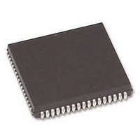
HD6473308RCP10V Renesas Electronics America, HD6473308RCP10V Datasheet - Page 104

HD6473308RCP10V
Manufacturer Part Number
HD6473308RCP10V
Description
MCU 5V 16K,PB-FREE 80-PLCC
Manufacturer
Renesas Electronics America
Series
H8® H8/330r
Datasheet
1.HD6473258P10V.pdf
(349 pages)
Specifications of HD6473308RCP10V
Core Size
8-Bit
Program Memory Size
16KB (16K x 8)
Oscillator Type
Internal
Core Processor
H8/300
Speed
10MHz
Number Of I /o
58
Program Memory Type
OTP
Ram Size
512 x 8
Operating Temperature
-20°C ~ 75°C
Package / Case
80-PLCC
No. Of I/o's
58
Ram Memory Size
512Byte
Cpu Speed
10MHz
No. Of Timers
3
No. Of Pwm Channels
2
Digital Ic Case
RoHS Compliant
Controller Family/series
H8/330
Peripherals
ADC
Rohs Compliant
Yes
Lead Free Status / RoHS Status
Lead free / RoHS Compliant
Voltage - Supply (vcc/vdd)
-
Eeprom Size
-
Data Converters
-
Peripherals
-
Connectivity
-
Lead Free Status / RoHS Status
Lead free / RoHS Compliant
Available stocks
Company
Part Number
Manufacturer
Quantity
Price
Company:
Part Number:
HD6473308RCP10V
Manufacturer:
Renesas Electronics America
Quantity:
10 000
- Current page: 104 of 349
- Download datasheet (2Mb)
Port 4 Data Register (P4DR)—H’FFB7
Bit
Initial value
Read/Write
P4DR is an 8-bit register containing the data for pins P4
output pins (P4DDR = "1") it reads the value in the P4DR latch, but for input pins (P4DDR = "0"),
it obtains the logic level directly from the pin, bypassing the P4DR latch. This also applies to pins
used for timer input or output.
MOS Pull-Ups: Are available for input pins, including timer input pins, in all modes. Software
can turn the MOS pull-up on by writing a “1” in P4DR, and turn it off by writing a “0.”
Pins P4
input or output, or input of 8-bit timer clock and reset signals. When a pin is used for timer signal
input, its P4DDR bit should normally be cleared to "0;" otherwise the timer will receive the value
in P4DR. If input pull-up is not desired, the P4DR bit should also be cleared to "0."
Pins P4
input or output, or for 8-bit timer output (P4
used for timer output are unaffected by the values in P4DDR and P4DR, and their MOS pull-ups
are automatically turned off.
Reset and Hardware Standby Mode: A reset or entry to the hardware standby mode clears
P4DDR and P4DR to all “0” and makes all pins into input port pins with the MOS pull-ups off.
Software Standby Mode: In the software standby mode, the control registers of the 8-bit and
PWM timers are initialized but P4DDR and P4DR remain in their previous states. All pins become
input or output port pins depending on the setting of P4DDR. Output pins output the values in
P4DR. The MOS pull-ups of input pins are on or off depending on the values in P4DR.
Figures 5-4 and 5-5 show schematic diagrams of port 4.
0
1
, P4
, P4
2
4
, P4
, P4
3
6
R/W
P4
, and P4
, and P4
7
0
7
5
7
R/W
: As indicated in Table 5-8, these pins can be used for general-purpose
: As indicated in Table 5-8, these pins can be used for general-purpose
P4
6
0
6
R/W
P4
5
0
5
1
and P4
R/W
89
P4
4
0
4
4
) or PWM timer output (P4
7
to P4
R/W
P4
3
0
3
0
. When the CPU reads P4DR, for
R/W
P4
2
0
2
R/W
P4
1
0
6
1
and P4
R/W
7
P4
). Pins
0
0
0
Related parts for HD6473308RCP10V
Image
Part Number
Description
Manufacturer
Datasheet
Request
R

Part Number:
Description:
KIT STARTER FOR M16C/29
Manufacturer:
Renesas Electronics America
Datasheet:

Part Number:
Description:
KIT STARTER FOR R8C/2D
Manufacturer:
Renesas Electronics America
Datasheet:

Part Number:
Description:
R0K33062P STARTER KIT
Manufacturer:
Renesas Electronics America
Datasheet:

Part Number:
Description:
KIT STARTER FOR R8C/23 E8A
Manufacturer:
Renesas Electronics America
Datasheet:

Part Number:
Description:
KIT STARTER FOR R8C/25
Manufacturer:
Renesas Electronics America
Datasheet:

Part Number:
Description:
KIT STARTER H8S2456 SHARPE DSPLY
Manufacturer:
Renesas Electronics America
Datasheet:

Part Number:
Description:
KIT STARTER FOR R8C38C
Manufacturer:
Renesas Electronics America
Datasheet:

Part Number:
Description:
KIT STARTER FOR R8C35C
Manufacturer:
Renesas Electronics America
Datasheet:

Part Number:
Description:
KIT STARTER FOR R8CL3AC+LCD APPS
Manufacturer:
Renesas Electronics America
Datasheet:

Part Number:
Description:
KIT STARTER FOR RX610
Manufacturer:
Renesas Electronics America
Datasheet:

Part Number:
Description:
KIT STARTER FOR R32C/118
Manufacturer:
Renesas Electronics America
Datasheet:

Part Number:
Description:
KIT DEV RSK-R8C/26-29
Manufacturer:
Renesas Electronics America
Datasheet:

Part Number:
Description:
KIT STARTER FOR SH7124
Manufacturer:
Renesas Electronics America
Datasheet:

Part Number:
Description:
KIT STARTER FOR H8SX/1622
Manufacturer:
Renesas Electronics America
Datasheet:

Part Number:
Description:
KIT DEV FOR SH7203
Manufacturer:
Renesas Electronics America
Datasheet:


