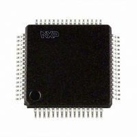
LPC2194JBD64,151 NXP Semiconductors, LPC2194JBD64,151 Datasheet - Page 16

LPC2194JBD64,151
Manufacturer Part Number
LPC2194JBD64,151
Description
IC ARM7 MCU FLASH 256K 64-LQFP
Manufacturer
NXP Semiconductors
Series
LPC2100r
Datasheet
1.LPC2194JBD64151.pdf
(33 pages)
Specifications of LPC2194JBD64,151
Core Processor
ARM7
Core Size
16/32-Bit
Speed
60MHz
Connectivity
CAN, I²C, Microwire, SPI, SSI, SSP, UART/USART
Peripherals
POR, PWM, WDT
Number Of I /o
46
Program Memory Size
256KB (256K x 8)
Program Memory Type
FLASH
Ram Size
16K x 8
Voltage - Supply (vcc/vdd)
1.65 V ~ 3.6 V
Data Converters
A/D 4x10b
Oscillator Type
Internal
Operating Temperature
-40°C ~ 105°C
Package / Case
64-LQFP
Lead Free Status / RoHS Status
Lead free / RoHS Compliant
Eeprom Size
-
Other names
568-1895
935275729151
LPC2194JBD64-S
935275729151
LPC2194JBD64-S
Available stocks
Company
Part Number
Manufacturer
Quantity
Price
Company:
Part Number:
LPC2194JBD64,151
Manufacturer:
NXP Semiconductors
Quantity:
10 000
Philips Semiconductors
9397 750 12757
Preliminary data
6.10.1 Features
6.10 General purpose parallel I/O
6.9 Pin function select register 2 (PINSEL2 - 0xE002C014)
Table 7:
The PINSEL2 register controls the functions of the pins as per the settings listed in
Table
function is selected for a pin. For other functions direction is controlled automatically.
Settings other than those shown in the table are reserved, and should not be used.
Table 8:
Device pins that are not connected to a specific peripheral function are controlled by
the GPIO registers. Pins may be dynamically configured as inputs or outputs.
Separate registers allow setting or clearing any number of outputs simultaneously.
The value of the output register may be read back, as well as the current state of the
port pins.
PINSEL1
27:26
29:28
31:30
PINSEL2 bits
1:0
2
3
31:4
31:30
•
•
•
Direction control of individual bits.
Separate control of output set and clear.
All I/O default to inputs after reset.
8. The direction control bit in the IODIR register is effective only when the GPIO
Pin function select register 1 (PINSEL1 - 0xE002C004)
Pin function select register 2 (PINSEL2 - 0xE002C014)
Pin Name
P0.29
P0.30
P0.31
Rev. 01 — 06 February 2004
Description
Reserved
When 0, pins P1.31:26 are GPIO pins. When 1,
P1.31:26 are used as Debug port.
When 0, pins P1.25:16 are used as GPIO pins. When
1, P1.25:16 are used as Trace port.
Reserved
Value
0
0
1
1
0
0
1
1
0
0
1
1
0
1
0
1
0
1
0
1
0
1
0
1
Single-chip 16/32-bit microcontrollers
Function
GPIO Port 0.29
AIN2 (A/D input 2)
Capture 0.3 (Timer0)
Match 0.3 (Timer0)
GPIO Port 0.30
AIN3 (A/D input 0)
EINT3
Capture 0.0 (Timer0)
Reserved
Reserved
Reserved
Reserved
© Koninklijke Philips Electronics N.V. 2004. All rights reserved.
…continued
LPC2194
Reset value
-
0
0
-
Value after
Reset
1
1
0
16 of 33


