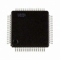
LPC2194JBD64,151 NXP Semiconductors, LPC2194JBD64,151 Datasheet - Page 21

LPC2194JBD64,151
Manufacturer Part Number
LPC2194JBD64,151
Description
IC ARM7 MCU FLASH 256K 64-LQFP
Manufacturer
NXP Semiconductors
Series
LPC2100r
Datasheet
1.LPC2194JBD64151.pdf
(33 pages)
Specifications of LPC2194JBD64,151
Core Processor
ARM7
Core Size
16/32-Bit
Speed
60MHz
Connectivity
CAN, I²C, Microwire, SPI, SSI, SSP, UART/USART
Peripherals
POR, PWM, WDT
Number Of I /o
46
Program Memory Size
256KB (256K x 8)
Program Memory Type
FLASH
Ram Size
16K x 8
Voltage - Supply (vcc/vdd)
1.65 V ~ 3.6 V
Data Converters
A/D 4x10b
Oscillator Type
Internal
Operating Temperature
-40°C ~ 105°C
Package / Case
64-LQFP
Lead Free Status / RoHS Status
Lead free / RoHS Compliant
Eeprom Size
-
Other names
568-1895
935275729151
LPC2194JBD64-S
935275729151
LPC2194JBD64-S
Available stocks
Company
Part Number
Manufacturer
Quantity
Price
Company:
Part Number:
LPC2194JBD64,151
Manufacturer:
NXP Semiconductors
Quantity:
10 000
Philips Semiconductors
9397 750 12757
Preliminary data
6.20.1 Crystal oscillator
6.20.2 PLL
6.20.3 Reset and wake-up timer
6.20 System control
The oscillator supports crystals in the range of 1 MHz to 30 MHz. The oscillator
output frequency is called f
as cclk for purposes of rate equations, etc. f
the PLL is running and connected. Refer to
information.
The PLL accepts an input clock frequency in the range of 10 MHz to 25 MHz. The
input frequency is multiplied up into the range of 10 MHz to 60 MHz with a Current
Controlled Oscillator (CCO). The multiplier can be an integer value from 1 to 32 (in
practice, the multiplier value cannot be higher than 6 on this family of microcontrollers
due to the upper frequency limit of the CPU). The CCO operates in the range of
156 MHz to 320 MHz, so there is an additional divider in the loop to keep the CCO
within its frequency range while the PLL is providing the desired output frequency.
The output divider may be set to divide by 2, 4, 8, or 16 to produce the output clock.
Since the minimum output divider value is 2, it is insured that the PLL output has a
50% duty cycle.The PLL is turned off and bypassed following a chip Reset and may
be enabled by software. The program must configure and activate the PLL, wait for
the PLL to Lock, then connect to the PLL as a clock source.
Reset has two sources on the LPC2194: the RESET pin and Watchdog Reset. The
RESET pin is a Schmitt trigger input pin with an additional glitch filter. Assertion of
chip Reset by any source starts the Wake-up Timer (see Wake-up Timer description
below), causing the internal chip reset to remain asserted until the external Reset is
de-asserted, the oscillator is running, a fixed number of clocks have passed, and the
on-chip Flash controller has completed its initialization.
When the internal Reset is removed, the processor begins executing at address 0,
which is the Reset vector. At that point, all of the processor and peripheral registers
have been initialized to predetermined values.
•
•
•
•
•
Pulse period and width can be any number of timer counts. This allows complete
flexibility in the trade-off between resolution and repetition rate. All PWM outputs
will occur at the same repetition rate.
Double edge controlled PWM outputs can be programmed to be either positive
going or negative going pulses.
Match register updates are synchronized with pulse outputs to prevent generation
of erroneous pulses. Software must ‘release’ new match values before they can
become effective.
May be used as a standard timer if the PWM mode is not enabled.
A 32-bit Timer/Counter with a programmable 32-bit Prescaler.
Rev. 01 — 06 February 2004
osc
and the ARM processor clock frequency is referred to
Section 6.20.2 “PLL”
osc
Single-chip 16/32-bit microcontrollers
and cclk are the same value unless
© Koninklijke Philips Electronics N.V. 2004. All rights reserved.
for additional
LPC2194
21 of 33


