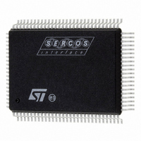
ST92F150JDV1QC STMicroelectronics, ST92F150JDV1QC Datasheet - Page 241

ST92F150JDV1QC
Manufacturer Part Number
ST92F150JDV1QC
Description
IC MCU 128K FLASH 100-PQFP
Manufacturer
STMicroelectronics
Series
ST9r
Datasheet
1.ST92F150CV1TB.pdf
(429 pages)
Specifications of ST92F150JDV1QC
Core Processor
ST9
Core Size
8/16-Bit
Speed
24MHz
Connectivity
CAN, I²C, LIN, SCI, SPI
Peripherals
DMA, LVD, POR, PWM, WDT
Number Of I /o
77
Program Memory Size
128KB (128K x 8)
Program Memory Type
FLASH
Eeprom Size
1K x 8
Ram Size
6K x 8
Voltage - Supply (vcc/vdd)
4.5 V ~ 5.5 V
Data Converters
A/D 16x10b
Oscillator Type
Internal
Operating Temperature
-40°C ~ 125°C
Package / Case
100-QFP
Processor Series
ST92F15x
Core
ST9
Data Bus Width
8 bit, 16 bit
Data Ram Size
6 KB
Interface Type
CAN, I2C, SCI, SPI
Maximum Clock Frequency
24 MHz
Number Of Programmable I/os
80
Number Of Timers
5 x 16 bit
Operating Supply Voltage
4.5 V to 5.5 V
Maximum Operating Temperature
+ 105 C
Mounting Style
SMD/SMT
Development Tools By Supplier
ST92F150-EPB
Minimum Operating Temperature
- 40 C
On-chip Adc
16 bit x 10 bit
Case
QFP
Lead Free Status / RoHS Status
Lead free / RoHS Compliant
Other names
497-2137
Available stocks
Company
Part Number
Manufacturer
Quantity
Price
- Current page: 241 of 429
- Download datasheet (8Mb)
ASYNCHRONOUS SERIAL COMMUNICATIONS INTERFACE (Cont’d)
10.6.4.3 Receiver
The SCI can receive data words of either 8 or 9
bits. When the M bit is set, word length is 9 bits
and the MSB is stored in the R8 bit in the SCICR1
register.
Character Reception
During a SCI reception, data shifts in least signifi-
cant bit first through the RDI pin. In this mode, the
SCIDR register consists or a buffer (RDR) be-
tween the internal bus and the received shift regis-
ter (see
Procedure
– Select the M bit to define the word length.
– Select the desired baud rate using the SCIBRR
– Set the RE bit, this enables the receiver which
When a character is received:
– The RDRF bit is set. It indicates that the content
– An interrupt is generated if the RIE bit is set and
– The error flags can be set if a frame error, noise
Clearing the RDRF bit is performed by the following
software sequence done by:
1. An access to the SCISR register
2. A read to the SCIDR register.
The RDRF bit must be cleared before the end of the
reception of the next character to avoid an overrun
error.
Break Character
When a break character is received, the SCI han-
dles it as a framing error.
Idle Character
When a idle frame is detected, there is the same
procedure as a data received character plus an
iterrupt if the ILIE bit is set and the IMI0 bit is set in
the SIMRH register.
and the SCIERPR registers.
begins searching for a start bit.
of the shift register is transferred to the RDR.
the IMI0 bit is set in the SIMRH register.
or an overrun error has been detected during re-
ception.
Figure
117).
ASYNCHRONOUS SERIAL COMMUNICATIONS INTERFACE (SCI-A)
Overrun Error
An overrun error occurs when a character is re-
ceived when RDRF has not been reset. Data can
not be transferred from the shift register to the
TDR register as long as the RDRF bit is not
cleared.
When a overrun error occurs:
– The OR bit is set.
– The RDR content will not be lost.
– The shift register will be overwritten.
– An interrupt is generated if the RIE bit is set and
The OR bit is reset by an access to the SCISR reg-
ister followed by a SCIDR register read operation.
Noise Error
Oversampling techniques are used for data recov-
ery by discriminating between valid incoming data
and noise.
When noise is detected in a frame:
– The NF is set at the rising edge of the RDRF bit.
– Data is transferred from the Shift register to the
– No interrupt is generated. However this bit rises
The NF bit is reset by a SCISR register read oper-
ation followed by a SCIDR register read operation.
Framing Error
A framing error is detected when:
– The stop bit is not recognized on reception at the
– A break is received.
When the framing error is detected:
– the FE bit is set by hardware
– Data is transferred from the Shift register to the
– No interrupt is generated. However this bit rises
The FE bit is reset by a SCISR register read oper-
ation followed by a SCIDR register read operation.
the IMI0 bit is set in the SIMRH register.
SCIDR register.
at the same time as the RDRF bit which itself
generates an interrupt.
expected time, following either a de-synchroni-
zation or excessive noise.
SCIDR register.
at the same time as the RDRF bit which itself
generates an interrupt.
241/429
9
Related parts for ST92F150JDV1QC
Image
Part Number
Description
Manufacturer
Datasheet
Request
R

Part Number:
Description:
BOARD PROGRAM FOR ST92F150 MCU
Manufacturer:
STMicroelectronics
Datasheet:

Part Number:
Description:
BOARD EVALUATION FOR ST9 SERIES
Manufacturer:
STMicroelectronics
Datasheet:

Part Number:
Description:
BOARD EMULATOR FOR ST9 SERIES
Manufacturer:
STMicroelectronics
Datasheet:

Part Number:
Description:
MCU, MPU & DSP Development Tools ST9 Dedication Board
Manufacturer:
STMicroelectronics
Datasheet:

Part Number:
Description:
STMicroelectronics [RIPPLE-CARRY BINARY COUNTER/DIVIDERS]
Manufacturer:
STMicroelectronics
Datasheet:

Part Number:
Description:
STMicroelectronics [LIQUID-CRYSTAL DISPLAY DRIVERS]
Manufacturer:
STMicroelectronics
Datasheet:

Part Number:
Description:
BOARD EVAL FOR MEMS SENSORS
Manufacturer:
STMicroelectronics
Datasheet:

Part Number:
Description:
NPN TRANSISTOR POWER MODULE
Manufacturer:
STMicroelectronics
Datasheet:

Part Number:
Description:
TURBOSWITCH ULTRA-FAST HIGH VOLTAGE DIODE
Manufacturer:
STMicroelectronics
Datasheet:

Part Number:
Description:
Manufacturer:
STMicroelectronics
Datasheet:

Part Number:
Description:
DIODE / SCR MODULE
Manufacturer:
STMicroelectronics
Datasheet:

Part Number:
Description:
DIODE / SCR MODULE
Manufacturer:
STMicroelectronics
Datasheet:


