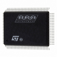
ST92F150JDV1QC STMicroelectronics, ST92F150JDV1QC Datasheet - Page 349

ST92F150JDV1QC
Manufacturer Part Number
ST92F150JDV1QC
Description
IC MCU 128K FLASH 100-PQFP
Manufacturer
STMicroelectronics
Series
ST9r
Datasheet
1.ST92F150CV1TB.pdf
(429 pages)
Specifications of ST92F150JDV1QC
Core Processor
ST9
Core Size
8/16-Bit
Speed
24MHz
Connectivity
CAN, I²C, LIN, SCI, SPI
Peripherals
DMA, LVD, POR, PWM, WDT
Number Of I /o
77
Program Memory Size
128KB (128K x 8)
Program Memory Type
FLASH
Eeprom Size
1K x 8
Ram Size
6K x 8
Voltage - Supply (vcc/vdd)
4.5 V ~ 5.5 V
Data Converters
A/D 16x10b
Oscillator Type
Internal
Operating Temperature
-40°C ~ 125°C
Package / Case
100-QFP
Processor Series
ST92F15x
Core
ST9
Data Bus Width
8 bit, 16 bit
Data Ram Size
6 KB
Interface Type
CAN, I2C, SCI, SPI
Maximum Clock Frequency
24 MHz
Number Of Programmable I/os
80
Number Of Timers
5 x 16 bit
Operating Supply Voltage
4.5 V to 5.5 V
Maximum Operating Temperature
+ 105 C
Mounting Style
SMD/SMT
Development Tools By Supplier
ST92F150-EPB
Minimum Operating Temperature
- 40 C
On-chip Adc
16 bit x 10 bit
Case
QFP
Lead Free Status / RoHS Status
Lead free / RoHS Compliant
Other names
497-2137
Available stocks
Company
Part Number
Manufacturer
Quantity
Price
- Current page: 349 of 429
- Download datasheet (8Mb)
CONTROLLER AREA NETWORK (Cont’d)
CAN BIT TIMING REGISTER 0 (CBTR0)
This register can only be accessed by the software
when the CAN hardware is in configuration mode.
Read / Write
Reset Value: 0000 0000 (00h)
Bit 7:6 SJW[1:0] Resynchronization Jump Width
These bits define the maximum number of time
quanta the CAN hardware is allowed to lengthen
or shorten a bit to perform the resynchronization.
Bit 5:0 BRP[5:0] Baud Rate Prescaler
These bits define the length of a time quantum.
tq = (BRP+1)/fsys
For more information on bit timing, please refer to
Section 10.10.5.7 Bit
CAN BIT TIMING REGISTER 1 (CBTR1)
Read / Write
Reset Value: 0001 0011 (23h)
Bit 7 = Reserved. Forced to 0 by hardware.
Bit 6:4 TS2[2:0] Time Segment 2
These bits define the number of time quanta in
Time Segment 2.
t
Bit 3:0 TS1[3:0] Time Segment 1
These bits define the number of time quanta in
Time Segment 1
t
.For more information on bit timing, please refer to
Section 10.10.5.7 Bit
BS2
BS1
SJW1 SJW0 BRP5
7
7
0
= t
= t
CAN
CAN
TS22
x (TS2[2:0] + 1),
x (TS1[3:0] + 1)
TS21
BRP4
TS20
Timing.
Timing.
BRP3
TS13
BRP2
TS12
BRP1
TS11
BRP0
TS10
0
0
CONTROLLER AREA NETWORK (bxCAN)
CAN FILTER PAGE SELECT REGISTER
(CFPSR)
All bits of this register are set and cleared by soft-
ware.
Read / Write
Reset Value: 0000 0000 (00h)
Bit 7:3 = Reserved. Forced to 0 by hardware.
Bit 2:0 = FPS[2:0] Filter Page Select
- Read/Write
This register contains the filter page number avail-
able in page 54.
Table 64. Filter Page Selection
FPS[2:0]
7
0
0
1
2
3
4
5
6
7
0
Acceptance Filter 0:1
Acceptance Filter 2:3
Acceptance Filter 4:5
Acceptance Filter 6:7
Filter Configuration
Filter Configuration
Filter Configuration
Filter Configuration
0
Filter Page Selected in Page 54
0
0
FPS2
FPS1
349/429
FPS0
0
9
Related parts for ST92F150JDV1QC
Image
Part Number
Description
Manufacturer
Datasheet
Request
R

Part Number:
Description:
BOARD PROGRAM FOR ST92F150 MCU
Manufacturer:
STMicroelectronics
Datasheet:

Part Number:
Description:
BOARD EVALUATION FOR ST9 SERIES
Manufacturer:
STMicroelectronics
Datasheet:

Part Number:
Description:
BOARD EMULATOR FOR ST9 SERIES
Manufacturer:
STMicroelectronics
Datasheet:

Part Number:
Description:
MCU, MPU & DSP Development Tools ST9 Dedication Board
Manufacturer:
STMicroelectronics
Datasheet:

Part Number:
Description:
STMicroelectronics [RIPPLE-CARRY BINARY COUNTER/DIVIDERS]
Manufacturer:
STMicroelectronics
Datasheet:

Part Number:
Description:
STMicroelectronics [LIQUID-CRYSTAL DISPLAY DRIVERS]
Manufacturer:
STMicroelectronics
Datasheet:

Part Number:
Description:
BOARD EVAL FOR MEMS SENSORS
Manufacturer:
STMicroelectronics
Datasheet:

Part Number:
Description:
NPN TRANSISTOR POWER MODULE
Manufacturer:
STMicroelectronics
Datasheet:

Part Number:
Description:
TURBOSWITCH ULTRA-FAST HIGH VOLTAGE DIODE
Manufacturer:
STMicroelectronics
Datasheet:

Part Number:
Description:
Manufacturer:
STMicroelectronics
Datasheet:

Part Number:
Description:
DIODE / SCR MODULE
Manufacturer:
STMicroelectronics
Datasheet:

Part Number:
Description:
DIODE / SCR MODULE
Manufacturer:
STMicroelectronics
Datasheet:


