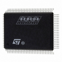
ST92F150JDV1QC STMicroelectronics, ST92F150JDV1QC Datasheet - Page 379

ST92F150JDV1QC
Manufacturer Part Number
ST92F150JDV1QC
Description
IC MCU 128K FLASH 100-PQFP
Manufacturer
STMicroelectronics
Series
ST9r
Datasheet
1.ST92F150CV1TB.pdf
(429 pages)
Specifications of ST92F150JDV1QC
Core Processor
ST9
Core Size
8/16-Bit
Speed
24MHz
Connectivity
CAN, I²C, LIN, SCI, SPI
Peripherals
DMA, LVD, POR, PWM, WDT
Number Of I /o
77
Program Memory Size
128KB (128K x 8)
Program Memory Type
FLASH
Eeprom Size
1K x 8
Ram Size
6K x 8
Voltage - Supply (vcc/vdd)
4.5 V ~ 5.5 V
Data Converters
A/D 16x10b
Oscillator Type
Internal
Operating Temperature
-40°C ~ 125°C
Package / Case
100-QFP
Processor Series
ST92F15x
Core
ST9
Data Bus Width
8 bit, 16 bit
Data Ram Size
6 KB
Interface Type
CAN, I2C, SCI, SPI
Maximum Clock Frequency
24 MHz
Number Of Programmable I/os
80
Number Of Timers
5 x 16 bit
Operating Supply Voltage
4.5 V to 5.5 V
Maximum Operating Temperature
+ 105 C
Mounting Style
SMD/SMT
Development Tools By Supplier
ST92F150-EPB
Minimum Operating Temperature
- 40 C
On-chip Adc
16 bit x 10 bit
Case
QFP
Lead Free Status / RoHS Status
Lead free / RoHS Compliant
Other names
497-2137
Available stocks
Company
Part Number
Manufacturer
Quantity
Price
- Current page: 379 of 429
- Download datasheet (8Mb)
AC ELECTRICAL CHARACTERISTICS
(V
specified)
Note:
All I/O Ports are configured in bidirectional weak pull-up mode with no DC load, unless otherwise specified, external clock is driven by a
square wave.
(1) Unless otherwise stated, typical data are based on V
(2) Current consumption to be added to IDD
(3) Value guaranteed by product characterization, not tested in production.
(4) Current consumption to be added to IDD
(5) The I/Os draw a transient current from V
or V
Symbol
I
I
I
DDLPWFI
I
I
I
DD
I
DDHALT
DDSTOP
I
DDRUN
DDOSC
DDRTC
I
ΔI
ΔI
ΔI
DDLPR
DDWFI
IN
DDTR
DD1
DD2
DD3
>V
= 5 V ± 10%, T
DD
-0.3V, it typically reaches its maximum value when V
Run Mode Current
FLASH/E
Supply Current
(Read)
FLASH/E
Supply Current
(Write/Erase)
Typical application
Run Mode Current
WFI Mode Current
FLASH/E
Supply Current
(Stand-by)
Main Voltage Regu-
lator Power
Consumption
Crystal Oscillator
Power Consump-
tion
Low Power WFI
Mode Current
RTC Mode Current
HALT Mode Cur-
rent
STOP Mode Cur-
rent
Input Transient I
Current
Parameter
(3)
(3)
(2)
(5)
3 TM
3 TM
3 TM
(4)
A
(2)
DD
=
–
40° C to +125° C for Max values and 25°C for Typ values, unless otherwise
CPU running with code execution
from RAM memory, all peripherals
in reset state, clock input (OSCIN)
driven by external square wave.
f
CPU running with code execution
from FLASH memory, all peripher-
als running in a typical configura-
tion, clock input (OSCIN) driven by
a 4-MHz crystal =
I
(Timers, CAN, etc)
FLASH/E
Main Voltage Regulator ON, I
PR
real time clock mode)
FLASH/E
Mode, Main Voltage Regulator
OFF, Standard Timer in Real Time
Clock mode
All I/O ports are configured in out-
put push-pull mode with no DC
load
DDRUN
f
INTCLK
INTCLK
+ I
DDOSC
RUN
LPWFI
DD
+ ΔI
in [MHz].
in [MHz].
3 TM
3 TM
when an input takes a voltage level in between V
Conditions
ST92F124/F150/F250 - ELECTRICAL CHARACTERISTICS
when the FLASH memory is accessed.
DD1
when the FLASH memory is in stand-by mode.
+ I
in Stand-by Mode,
in Power-Down
DD (Standard Timer in
+ I
DD Peripherals
DD
= 5V. They are only reported for design guide lines not tested in production.
IN
is approximatively at V
DDL-
4MHz / 32
4MHz / 32
frequency
frequency
INTCLK
24 MHz
24 MHz
24 MHz
any
any
-
-
-
-
-
-
DD
see
1.8xf
/2.
Figure 159
Typ
INTCLK
2.5 +
300
200
550
250
300
SS
45
12
50
14
20
2
5
and V
(1)
/MHz
(3)
DD
. This current is 0 for V
0.9xf
INTCLK
Max
1000
60
22
25
/MHz
(3)
379/429
IN
<0.3V
Unit
mA
mA
mA
mA
mA
mA
mA
μA
μA
μA
μA
μA
μA
μA
μA
1
Related parts for ST92F150JDV1QC
Image
Part Number
Description
Manufacturer
Datasheet
Request
R

Part Number:
Description:
BOARD PROGRAM FOR ST92F150 MCU
Manufacturer:
STMicroelectronics
Datasheet:

Part Number:
Description:
BOARD EVALUATION FOR ST9 SERIES
Manufacturer:
STMicroelectronics
Datasheet:

Part Number:
Description:
BOARD EMULATOR FOR ST9 SERIES
Manufacturer:
STMicroelectronics
Datasheet:

Part Number:
Description:
MCU, MPU & DSP Development Tools ST9 Dedication Board
Manufacturer:
STMicroelectronics
Datasheet:

Part Number:
Description:
STMicroelectronics [RIPPLE-CARRY BINARY COUNTER/DIVIDERS]
Manufacturer:
STMicroelectronics
Datasheet:

Part Number:
Description:
STMicroelectronics [LIQUID-CRYSTAL DISPLAY DRIVERS]
Manufacturer:
STMicroelectronics
Datasheet:

Part Number:
Description:
BOARD EVAL FOR MEMS SENSORS
Manufacturer:
STMicroelectronics
Datasheet:

Part Number:
Description:
NPN TRANSISTOR POWER MODULE
Manufacturer:
STMicroelectronics
Datasheet:

Part Number:
Description:
TURBOSWITCH ULTRA-FAST HIGH VOLTAGE DIODE
Manufacturer:
STMicroelectronics
Datasheet:

Part Number:
Description:
Manufacturer:
STMicroelectronics
Datasheet:

Part Number:
Description:
DIODE / SCR MODULE
Manufacturer:
STMicroelectronics
Datasheet:

Part Number:
Description:
DIODE / SCR MODULE
Manufacturer:
STMicroelectronics
Datasheet:


