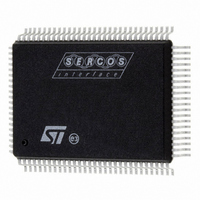
ST92F150JDV1QC STMicroelectronics, ST92F150JDV1QC Datasheet - Page 280

ST92F150JDV1QC
Manufacturer Part Number
ST92F150JDV1QC
Description
IC MCU 128K FLASH 100-PQFP
Manufacturer
STMicroelectronics
Series
ST9r
Datasheet
1.ST92F150CV1TB.pdf
(429 pages)
Specifications of ST92F150JDV1QC
Core Processor
ST9
Core Size
8/16-Bit
Speed
24MHz
Connectivity
CAN, I²C, LIN, SCI, SPI
Peripherals
DMA, LVD, POR, PWM, WDT
Number Of I /o
77
Program Memory Size
128KB (128K x 8)
Program Memory Type
FLASH
Eeprom Size
1K x 8
Ram Size
6K x 8
Voltage - Supply (vcc/vdd)
4.5 V ~ 5.5 V
Data Converters
A/D 16x10b
Oscillator Type
Internal
Operating Temperature
-40°C ~ 125°C
Package / Case
100-QFP
Processor Series
ST92F15x
Core
ST9
Data Bus Width
8 bit, 16 bit
Data Ram Size
6 KB
Interface Type
CAN, I2C, SCI, SPI
Maximum Clock Frequency
24 MHz
Number Of Programmable I/os
80
Number Of Timers
5 x 16 bit
Operating Supply Voltage
4.5 V to 5.5 V
Maximum Operating Temperature
+ 105 C
Mounting Style
SMD/SMT
Development Tools By Supplier
ST92F150-EPB
Minimum Operating Temperature
- 40 C
On-chip Adc
16 bit x 10 bit
Case
QFP
Lead Free Status / RoHS Status
Lead free / RoHS Compliant
Other names
497-2137
Available stocks
Company
Part Number
Manufacturer
Quantity
Price
- Current page: 280 of 429
- Download datasheet (8Mb)
I2C BUS INTERFACE
I
INTERRUPT VECTOR REGISTER (I2CIVR)
R249 - Read / Write
Register Page: 20 (I2C_0) or 22 (I2C_1)
Reset Value: Undefined
Bits 7:3 = V[7:3] Interrupt Vector Base Address.
User programmable interrupt vector bits. These
are the five more significant bits of the interrupt
vector base address. They must be set before en-
abling the interrupt features.
Bits 2:1 = EV[2:1] Encoded Interrupt Source.
These Read-Only bits are set by hardware accord-
ing to the interrupt source:
– 01: error condition detected
– 10: data received
– 11: peripheral ready to transmit
Bit 0 = Reserved.
Forced by hardware to 0.
RECEIVER DMA SOURCE ADDRESS POINTER
REGISTER (I2CRDAP)
R250 - Read / Write
Register Page: 20 (I2C_0) or 22 (I2C_1)
Reset Value: Undefined
Bits 7:1 = RA[7:1] Receiver DMA Address Pointer.
I2CRDAP contains the address of the pointer (in
the Register File) of the Receiver DMA data
source when the DMA is selected between the
peripheral and the Memory Space. Otherwise,
280/429
9
2
RA7 RA6 RA5 RA4 RA3 RA2 RA1
C BUS INTERFACE (Cont’d)
V7
7
7
V6
V5
V4
V3
EV2
EV1
RPS
0
0
0
(DMA between peripheral and Register file), this
register has no meaning.
See
of this register.
Bit 0 = RPS Receiver DMA Memory Pointer Selec-
tor.
If memory has been selected for DMA transfer
(I2CRDC.RF/MEM = 0) then:
0: Select ISR register for Receiver DMA transfer
1: Select DMASR register for Receiver DMA trans-
RECEIVER DMA TRANSACTION COUNTER
REGISTER (I2CRDC)
R251 - Read / Write
Register Page: 20 (I2C_0) or 22 (I2C_1)
Reset Value: Undefined
Bits 7:1 = RC[7:1] Receiver DMA Counter Pointer.
I2CRDC contains the address of the pointer (in the
Register File) of the DMA receiver transaction
counter when the DMA between Peripheral and
Memory Space is selected. Otherwise (DMA be-
tween Peripheral and Register File), this register
points to a pair of registers that are used as DMA
Address register and DMA Transaction Counter.
See
more details on the use of this register.
Bit 0 = RF/MEM Receiver Register File/ Memory
Selector.
0: DMA towards Memory
1: DMA towards Register file
RC7 RC6 RC5 RC4 RC3 RC2 RC1 RF/MEM
address extension.
fer address extension.
7
Section 10.8.6.1
Section 10.8.6.1
for more details on the use
and
Section 10.8.6.2
0
for
Related parts for ST92F150JDV1QC
Image
Part Number
Description
Manufacturer
Datasheet
Request
R

Part Number:
Description:
BOARD PROGRAM FOR ST92F150 MCU
Manufacturer:
STMicroelectronics
Datasheet:

Part Number:
Description:
BOARD EVALUATION FOR ST9 SERIES
Manufacturer:
STMicroelectronics
Datasheet:

Part Number:
Description:
BOARD EMULATOR FOR ST9 SERIES
Manufacturer:
STMicroelectronics
Datasheet:

Part Number:
Description:
MCU, MPU & DSP Development Tools ST9 Dedication Board
Manufacturer:
STMicroelectronics
Datasheet:

Part Number:
Description:
STMicroelectronics [RIPPLE-CARRY BINARY COUNTER/DIVIDERS]
Manufacturer:
STMicroelectronics
Datasheet:

Part Number:
Description:
STMicroelectronics [LIQUID-CRYSTAL DISPLAY DRIVERS]
Manufacturer:
STMicroelectronics
Datasheet:

Part Number:
Description:
BOARD EVAL FOR MEMS SENSORS
Manufacturer:
STMicroelectronics
Datasheet:

Part Number:
Description:
NPN TRANSISTOR POWER MODULE
Manufacturer:
STMicroelectronics
Datasheet:

Part Number:
Description:
TURBOSWITCH ULTRA-FAST HIGH VOLTAGE DIODE
Manufacturer:
STMicroelectronics
Datasheet:

Part Number:
Description:
Manufacturer:
STMicroelectronics
Datasheet:

Part Number:
Description:
DIODE / SCR MODULE
Manufacturer:
STMicroelectronics
Datasheet:

Part Number:
Description:
DIODE / SCR MODULE
Manufacturer:
STMicroelectronics
Datasheet:


