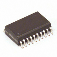
MC68HC908JB8JDW Freescale Semiconductor, MC68HC908JB8JDW Datasheet - Page 135

MC68HC908JB8JDW
Manufacturer Part Number
MC68HC908JB8JDW
Description
IC MCU 8K FLASH 3MHZ 20-SOIC
Manufacturer
Freescale Semiconductor
Series
HC08r
Datasheet
1.MC908JB8JDWE.pdf
(286 pages)
Specifications of MC68HC908JB8JDW
Core Processor
HC08
Core Size
8-Bit
Speed
3MHz
Connectivity
USB
Peripherals
LVD, POR, PWM
Number Of I /o
13
Program Memory Size
8KB (8K x 8)
Program Memory Type
FLASH
Ram Size
256 x 8
Voltage - Supply (vcc/vdd)
4 V ~ 5.5 V
Oscillator Type
Internal
Operating Temperature
0°C ~ 70°C
Package / Case
20-SOIC (7.5mm Width)
Lead Free Status / RoHS Status
Contains lead / RoHS non-compliant
Eeprom Size
-
Data Converters
-
Available stocks
Company
Part Number
Manufacturer
Quantity
Price
Part Number:
MC68HC908JB8JDW
Manufacturer:
MOTOROLA/摩托罗拉
Quantity:
20 000
Company:
Part Number:
MC68HC908JB8JDWE
Manufacturer:
VISHAY
Quantity:
6 700
Part Number:
MC68HC908JB8JDWE
Manufacturer:
FREESCALE
Quantity:
20 000
- Current page: 135 of 286
- Download datasheet (2Mb)
9.7.2.3 Receiver Data Jitter
9.7.2.4 Data Source Jitter
MC68HC908JB8•MC68HC08JB8•MC68HC08JT8 — Rev. 2.3
Freescale Semiconductor
The receiver features an input sensitivity of 200mV when both
differential data inputs are in the differential common mode range of
0.8V to 2.5V as shown in
receiver, there is a single-ended receiver (schmitt trigger) for each of the
two data lines.
The data receivers for all types of devices must be able to properly
decode the differential data in the presence of jitter. The more of the bit
time that any data edge can occupy and still be decoded, the more
reliable the data transfer will be. Data receivers are required to decode
differential data transitions that occur in a window plus and minus a
nominal quarter bit time from the nominal (centered) data edge position.
Jitter will be caused by the delay mismatches and by mismatches in the
source and destination data rates (frequencies). The receive data jitter
budget for low speed is given in
The specification includes the consecutive (next) and paired transition
values for each source of jitter.
The source of data can have some variation (jitter) in the timing of edges
of the data transmitted. The time between any set of data transitions is
N × T
transitions and T
The data jitter is measured with the same capacitive load used for
maximum rise and fall times and is measured at the crossover points of
the data lines as shown in
–1.0
Period
0.0
Universal Serial Bus Module (USB)
Figure 9-12. Differential Input Sensitivity Range
0.2
±
jitter time, where N is the number of bits between the
0.4
Period
0.6
0.8
is defined as the actual period of the data rate.
1.0
Figure
Figure
INPUT VOLTAGE RANGE (VOLTS)
Differential Input voltage Range
1.2
Differential Output
1.4
Section 18. Electrical
Voltage Range
9-12. In addition to the differential
Crossover
9-13.
1.6
1.8
2.0
Universal Serial Bus Module (USB)
2.2
2.4
2.6
Hardware Description
Specifications.
2.8
3.0
Technical Data
3.2
5.5
135
Related parts for MC68HC908JB8JDW
Image
Part Number
Description
Manufacturer
Datasheet
Request
R
Part Number:
Description:
Manufacturer:
Freescale Semiconductor, Inc
Datasheet:
Part Number:
Description:
Manufacturer:
Freescale Semiconductor, Inc
Datasheet:
Part Number:
Description:
Manufacturer:
Freescale Semiconductor, Inc
Datasheet:
Part Number:
Description:
Manufacturer:
Freescale Semiconductor, Inc
Datasheet:
Part Number:
Description:
Manufacturer:
Freescale Semiconductor, Inc
Datasheet:
Part Number:
Description:
Manufacturer:
Freescale Semiconductor, Inc
Datasheet:
Part Number:
Description:
Manufacturer:
Freescale Semiconductor, Inc
Datasheet:
Part Number:
Description:
Manufacturer:
Freescale Semiconductor, Inc
Datasheet:
Part Number:
Description:
Manufacturer:
Freescale Semiconductor, Inc
Datasheet:
Part Number:
Description:
Manufacturer:
Freescale Semiconductor, Inc
Datasheet:
Part Number:
Description:
Manufacturer:
Freescale Semiconductor, Inc
Datasheet:
Part Number:
Description:
Manufacturer:
Freescale Semiconductor, Inc
Datasheet:
Part Number:
Description:
Manufacturer:
Freescale Semiconductor, Inc
Datasheet:
Part Number:
Description:
Manufacturer:
Freescale Semiconductor, Inc
Datasheet:
Part Number:
Description:
Manufacturer:
Freescale Semiconductor, Inc
Datasheet:


