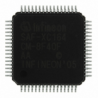
SAF-XC164CM-8F40F AA Infineon Technologies, SAF-XC164CM-8F40F AA Datasheet - Page 12

SAF-XC164CM-8F40F AA
Manufacturer Part Number
SAF-XC164CM-8F40F AA
Description
IC MCU 16BIT FLASH TQFP-64-8
Manufacturer
Infineon Technologies
Series
XC16xr
Datasheet
1.SAF-XC164CM-4F20F_AA.pdf
(70 pages)
Specifications of SAF-XC164CM-8F40F AA
Core Processor
C166SV2
Core Size
16-Bit
Speed
40MHz
Connectivity
CAN, SPI, UART/USART
Peripherals
PWM, WDT
Number Of I /o
47
Program Memory Size
64KB (64K x 8)
Program Memory Type
FLASH
Ram Size
6K x 8
Voltage - Supply (vcc/vdd)
2.35 V ~ 2.7 V
Data Converters
A/D 14x8/10b
Oscillator Type
Internal
Operating Temperature
-40°C ~ 85°C
Package / Case
64-LFQFP
Data Bus Width
16 bit
Data Ram Size
6 KB
Interface Type
2xASC, 2xSSC
Maximum Clock Frequency
40 MHz
Number Of Programmable I/os
47
Number Of Timers
9
Operating Supply Voltage
5 V
Maximum Operating Temperature
+ 85 C
Mounting Style
SMD/SMT
Minimum Operating Temperature
- 40 C
On-chip Adc
10 bit, 14 Channel
Packages
PG-LQFP-64
Max Clock Frequency
40.0 MHz
Sram (incl. Cache)
6.0 KByte
Can Nodes
2
A / D Input Lines (incl. Fadc)
14
Program Memory
64.0 KByte
For Use With
B158-H8961-X-X-7600IN - KIT EASY XC164CMXC164CMUCANIN - KIT U-CAN STARTER XC164CMMCBX167-NET - BOARD EVAL INFINEON CAN/ETHRNTMCBXC167-BASIC - BOARD EVAL BASIC INFINEON XC16X
Lead Free Status / RoHS Status
Lead free / RoHS Compliant
Eeprom Size
-
Lead Free Status / Rohs Status
Details
Other names
SAF-XC164CM-8F40FAACT
SAF-XC164CM-8F40FAACT
SAF-XC164CM-8F40FAAINCT
SAF-XC164CM-8F40FAACT
SAF-XC164CM-8F40FAAINCT
Table 2
Sym-
bol
Port 5
P5.0
P5.1
P5.2
P5.3
P5.4
P5.5
P5.10
P5.11
P5.6
P5.7
P5.12
P5.13
P5.14
P5.15
TRST
Data Sheet
Pin
Num.
9-18,
21-24
9
10
11
12
13
14
15
16
17
18
21
22
23
24
62
Pin Definitions and Functions (cont’d)
Input
Outp.
I
I
I
I
I
I
I
I
I
I
I
I
I
I
I
I
Function
Port 5 is a 14-bit input-only port.
The pins of Port 5 also serve as analog input channels for the
A/D converter, or they serve as timer inputs:
AN0
AN1
AN2
AN3
AN4
AN5
AN10 (T6EUD): GPT2 Timer T6 Ext. Up/Down Ctrl. Inp.
AN11 (T5EUD): GPT2 Timer T5 Ext. Up/Down Ctrl. Inp.
AN6
AN7
AN12 (T6IN): GPT2 Timer T6 Count/Gate Input
AN13 (T5IN): GPT2 Timer T5 Count/Gate Input
AN14 (T4EUD): GPT1 Timer T4 Ext. Up/Down Ctrl. Inp.
AN15 (T2EUD): GPT1 Timer T2 Ext. Up/Down Ctrl. Inp.
Test-System Reset Input. For normal system operation, pin
TRST should be held low. A high level at this pin at the rising
edge of RSTIN enables the hardware configuration and
activates the XC164CM’s debug system. In this case, pin
TRST must be driven low once to reset the debug system.
10
General Device Information
Derivatives
V1.4, 2007-03
XC164CM


