FDS8958A_F085 Fairchild Semiconductor, FDS8958A_F085 Datasheet
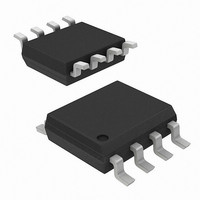
MOSFET N/P-CH 30V DUAL 8-SOIC

FDS8958A_F085

Manufacturer Part Number
FDS8958A_F085
Description
MOSFET N/P-CH 30V DUAL 8-SOIC
Manufacturer
Fairchild Semiconductor
Series
PowerTrench®r
Datasheet

Specifications of FDS8958A_F085

Fet Type
N and P-Channel
Fet Feature
Logic Level Gate
Rds On (max) @ Id, Vgs
28 mOhm @ 7A, 10V
Drain To Source Voltage (vdss)
30V
Current - Continuous Drain (id) @ 25° C
7A, 5A
Vgs(th) (max) @ Id
3V @ 250µA
Gate Charge (qg) @ Vgs
16nC @ 10V
Input Capacitance (ciss) @ Vds
575pF @ 15V
Power - Max
900mW
Mounting Type
Surface Mount
Package / Case
*
Configuration
Dual
Transistor Polarity
N and P-Channel
Resistance Drain-source Rds (on)
19 mOhms, 42 mOhms
Forward Transconductance Gfs (max / Min)
25 S, 10 S
Drain-source Breakdown Voltage
30 V
Gate-source Breakdown Voltage
20 V
Continuous Drain Current
7 A, - 5 A
Power Dissipation
2 W
Maximum Operating Temperature
+ 150 C
Mounting Style
SMD/SMT
Lead Free Status / RoHS Status
Lead free / RoHS Compliant
Other names
FDS8958A_F085TR

Available stocks

Company
Part Number
Manufacturer
Quantity
Price
Part Number:
FDS8958A_F085FDS8958A-F085
Manufacturer:
ON/安森美
Quantity:
20 000
Part Number:
FDS8958A_F085FDS8958A-F085
0
Company:
Part Number:
FDS8958A_F085FDS8958A-F085
Quantity:
5 000
©2010 Fairchild Semiconductor Corporation
FDS8958A_F085 Rev. A
FDS8958A_F085
Dual N & P-Channel PowerTrench
General Description
These dual N- and P-Channel enhancement mode
power field effect transistors are produced using
Fairchild
process that has been especially tailored to minimize
on-state ressitance and yet maintain superior switching
performance.
These devices are well suited for low voltage and
battery powered applications where low in-line power
loss and fast switching are required.
Absolute Maximum Ratings
V
V
I
P
E
T
Thermal Characteristics
R
R
Package Marking and Ordering Information
Symbol
D
DSS
GSS
D
AS
J
θJA
θJC
, T
Device Marking
STG
FDS8958A
Semiconductor’s
SO-8
Drain-Source Voltage
Gate-Source Voltage
Drain Current
Power Dissipation for Dual Operation
Power Dissipation for Single Operation
Single Pulse Avalanche Energy
Operating and Storage Junction Temperature Range
Thermal Resistance, Junction-to-Ambient
Thermal Resistance, Junction-to-Case
D
D1
Pin 1
D
D1
SO-8
D
FDS8958A_F085
advanced
D2
- Continuous
- Pulsed
D
D2
Device
Parameter
S1
S
G1
PowerTrench
S
S2
S
G2
T
G
A
= 25°C unless otherwise noted
® ® ® ®
Reel Size
MOSFET
13”
1
(Note 1a)
(Note 1a)
(Note 1c)
(Note 3)
(Note 1a)
(Note 1)
Features
Qualified to AEC Q101
RoHS Compliant
Q1:
7.0A, 30V
Q2:
-5A, -30V
Fast switching speed
High power and handling capability in a widely
used surface mount package
N-Channel
P-Channel
Q1
±20
1.6
0.9
5
6
7
8
30
20
54
7
2
Tape width
-55 to +150
R
R
R
R
12mm
DS(on)
DS(on)
DS(on)
DS(on)
Q2
Q1
78
40
= 0.028Ω @ V
= 0.040Ω @ V
= 0.052Ω @ V
= 0.080Ω @ V
Q2
±20
-20
1.6
0.9
30
13
-5
2
February 2010
4
3
2
1
www.fairchildsemi.com
GS
GS
GS
GS
2500 units
Quantity
= 10V
= 4.5V
= -10V
= -4.5V
Units
°C/W
°C/W
mJ
°C
W
V
V
A
tm

Related parts for FDS8958A_F085

FDS8958A_F085 Summary of contents

Page 1

... Thermal Characteristics Thermal Resistance, Junction-to-Ambient R θJA Thermal Resistance, Junction-to-Case R θJC Package Marking and Ordering Information Device Marking Device FDS8958A FDS8958A_F085 ©2010 Fairchild Semiconductor Corporation FDS8958A_F085 Rev. A ® ® ® ® MOSFET Features • Q1: N-Channel 7.0A, 30V PowerTrench • Q2: P-Channel -5A, -30V • ...

Page 2

... I On-State Drain Current D(on) g Forward Transconductance FS Dynamic Characteristics C Input Capacitance iss C Output Capacitance oss C Reverse Transfer Capacitance rss R Gate Resistance G FDS8958A_F085 Rev 25°C unless otherwise noted A Test Conditions Type Min Typ Max Units = 250 µ -250 µ 250 µA, Referenced to 25°C ...

Page 3

... Scale letter size paper 2. Pulse Test: Pulse Width < 300µs, Duty Cycle < 2.0% 3. Starting TJ = 25° 3mH 6A 30V Starting TJ = 25° 3mH 3A 30V FDS8958A_F085 Rev. A (continued 25°C unless otherwise noted A Test Conditions (Note Ω 10V GEN ...

Page 4

... T , JUNCTION TEMPERATURE ( J Figure 3. On-Resistance Variation with Temperature 125 1 GATE TO SOURCE VOLTAGE (V) GS Figure 5. Transfer Characteristics. FDS8958A_F085 Rev. A 2.2 3.5V 1 1.4 3.0V 1 0.6 1 Figure 2. On-Resistance Variation with Drain Current and Gate Voltage. 0.08 0.07 0.06 0.05 0.04 0. 0.02 0.01 75 100 ...

Page 5

... R = 135 C/W θ 0.01 0 DRAIN-SOURCE VOLTAGE (V) DS Figure 9. Maximum Safe Operating Area 0.001 0.01 Figure 11. Single Pulse Maximum Power Dissipation. FDS8958A_F085 Rev. A 800 V = 10V 20V DS 600 15V 400 200 C rss Figure 8. Capacitance Characteristics. 10 100µs 1ms 10ms 1 0.01 10 100 Figure 10. Unclamped Inductive Switching ...

Page 6

... T , JUNCTION TEMPERATURE ( J Figure 14. On-Resistance Variation with Temperature - 1 GATE TO SOURCE VOLTAGE (V) GS Figure 16. Transfer Characteristics. FDS8958A_F085 Rev 1.8 -4.5V 1.6 -4.0V 1.4 1.2 -3.5V 1 -3.0V 0 Figure 13. On-Resistance Variation with Drain Current and Gate Voltage. 0.25 0.2 0. 100 ...

Page 7

... SINGLE PULSE 0.001 0.0001 0.001 Figure 23. Transient Thermal Response Curve. Thermal characterization performed using the conditions described in Note 1c. Transient thermal response will change depending on the circuit board design. FDS8958A_F085 Rev. A 0.01 0 TIME (sec ( 135 °C/W ...

Page 8

... Datasheet Identification Product Status Advance Information Formative / In Design Preliminary First Production No Identification Needed Full Production Obsolete Not In Production FDS8958A_F085 Rev. A ® FRFET PowerTrench SM Global Power Resource PowerXS™ Green FPS™ Programmable Active Droop™ ® Green FPS™ e-Series™ ...

Related keywords