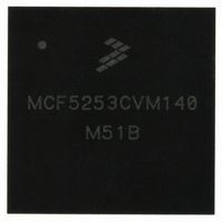
MCF5253CVM140 Freescale Semiconductor, MCF5253CVM140 Datasheet - Page 204

MCF5253CVM140
Manufacturer Part Number
MCF5253CVM140
Description
IC MPU 32BIT 140MHZ 225-MAPBGA
Manufacturer
Freescale Semiconductor
Series
MCF525xr
Datasheets
1.MCF5253VM140J.pdf
(34 pages)
2.MCF5253VM140J.pdf
(8 pages)
3.MCF5253VM140J.pdf
(648 pages)
4.MCF5253VM140J.pdf
(2 pages)
Specifications of MCF5253CVM140
Core Processor
Coldfire V2
Core Size
32-Bit
Speed
140MHz
Connectivity
CAN, EBI/EMI, I²C, QSPI, UART/USART, USB OTG
Peripherals
DMA, WDT
Program Memory Type
ROMless
Ram Size
128K x 8
Voltage - Supply (vcc/vdd)
1.08 V ~ 1.32 V
Data Converters
A/D 6x12b
Oscillator Type
External
Operating Temperature
-40°C ~ 85°C
Package / Case
225-MAPBGA
Family Name
MCF5xxx
Device Core
ColdFire V2
Device Core Size
32b
Frequency (max)
140MHz
Instruction Set Architecture
RISC
Supply Voltage 1 (typ)
1.2/3.3V
Operating Supply Voltage (max)
1.32/3.6V
Operating Supply Voltage (min)
1.08/3V
Operating Temp Range
-40C to 85C
Operating Temperature Classification
Industrial
Mounting
Surface Mount
Pin Count
225
Package Type
MA-BGA
Lead Free Status / RoHS Status
Lead free / RoHS Compliant
Number Of I /o
-
Eeprom Size
-
Program Memory Size
-
Lead Free Status / Rohs Status
Compliant
Available stocks
Company
Part Number
Manufacturer
Quantity
Price
Company:
Part Number:
MCF5253CVM140
Manufacturer:
FREESCALE
Quantity:
300
Company:
Part Number:
MCF5253CVM140
Manufacturer:
Freescale Semiconductor
Quantity:
10 000
Part Number:
MCF5253CVM140
Manufacturer:
FREESCALE
Quantity:
20 000
Company:
Part Number:
MCF5253CVM140J
Manufacturer:
Freescale Semiconductor
Quantity:
10 000
- MCF5253VM140J PDF datasheet
- MCF5253VM140J PDF datasheet #2
- MCF5253VM140J PDF datasheet #3
- MCF5253VM140J PDF datasheet #4
- Current page: 204 of 648
- Download datasheet (8Mb)
IDE and Flash Media Interface
13.1.3
Dedicated logic has been added to the MCF5253 to allow IDE compliant cycles on the bus. The logic can
generate the transfer acknowledge (TA) signal for CS2 access. The manner in which the TA signal is
generated is programmable using the IDE config 2 register, and is compatible with IDE/SmartMedia
requirements.
The timing diagram for a non-IORDY controlled IDE/SmartMedia TA generation is shown in
13-6
IORDY ENABLE 2
IORDY ENABLE 3
WAITCOUNT2
WAITCOUNT3
MBAR2 + 0x190
TA ENABLE 2
TA ENABLE 3
Address
dior
(writes disabled)
dior
(writes enabled)
Field
15–8
DIOR
DIOR
DIOW
7–0
19
18
17
16
CS2 pin
CS3 pin
sre
(writes enabled)
RWb
Cycle Termination on CS2 (IDE_DIOR, IDE_DIOW)
diow
SRE
sre
(writes disabled)
SWE
SRE
swe
1 Allow IORDY to delay TA generation for CS2
0 Do not look at IORDY for CS2 TA generation
1 Generate TA for CS2 accesses
0 Do not generate TA for CS2
Reserved set to 0
Reserved set to 0
CS2 delay count. Controls TA timing for read cycles
CS2 delay count. Controls TA timing for write cycles
Access
RW
Table 13-4. IDEConfig2 Register Field Description
Figure 13-3. IDE_DIOR Timing Diagram
Size
Bits
Table 13-3. IDEConfig2 Register
32
MCF5253 Reference Manual, Rev. 1
IDE config2
Name
Description
Configuration of TA generation on CS2
Description
Freescale Semiconductor
Figure 13-4
RES
0
0
0
0
0
0
Related parts for MCF5253CVM140
Image
Part Number
Description
Manufacturer
Datasheet
Request
R
Part Number:
Description:
Mcf5253 Coldfire? Microprocessor Data Sheet
Manufacturer:
Freescale Semiconductor, Inc
Datasheet:
Part Number:
Description:
Manufacturer:
Freescale Semiconductor, Inc
Datasheet:
Part Number:
Description:
Manufacturer:
Freescale Semiconductor, Inc
Datasheet:
Part Number:
Description:
Manufacturer:
Freescale Semiconductor, Inc
Datasheet:
Part Number:
Description:
Manufacturer:
Freescale Semiconductor, Inc
Datasheet:
Part Number:
Description:
Manufacturer:
Freescale Semiconductor, Inc
Datasheet:
Part Number:
Description:
Manufacturer:
Freescale Semiconductor, Inc
Datasheet:
Part Number:
Description:
Manufacturer:
Freescale Semiconductor, Inc
Datasheet:
Part Number:
Description:
Manufacturer:
Freescale Semiconductor, Inc
Datasheet:
Part Number:
Description:
Manufacturer:
Freescale Semiconductor, Inc
Datasheet:
Part Number:
Description:
Manufacturer:
Freescale Semiconductor, Inc
Datasheet:
Part Number:
Description:
Manufacturer:
Freescale Semiconductor, Inc
Datasheet:
Part Number:
Description:
Manufacturer:
Freescale Semiconductor, Inc
Datasheet:
Part Number:
Description:
Manufacturer:
Freescale Semiconductor, Inc
Datasheet:
Part Number:
Description:
Manufacturer:
Freescale Semiconductor, Inc
Datasheet:


