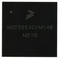
MCF5253CVM140 Freescale Semiconductor, MCF5253CVM140 Datasheet - Page 349

MCF5253CVM140
Manufacturer Part Number
MCF5253CVM140
Description
IC MPU 32BIT 140MHZ 225-MAPBGA
Manufacturer
Freescale Semiconductor
Series
MCF525xr
Datasheets
1.MCF5253VM140J.pdf
(34 pages)
2.MCF5253VM140J.pdf
(8 pages)
3.MCF5253VM140J.pdf
(648 pages)
4.MCF5253VM140J.pdf
(2 pages)
Specifications of MCF5253CVM140
Core Processor
Coldfire V2
Core Size
32-Bit
Speed
140MHz
Connectivity
CAN, EBI/EMI, I²C, QSPI, UART/USART, USB OTG
Peripherals
DMA, WDT
Program Memory Type
ROMless
Ram Size
128K x 8
Voltage - Supply (vcc/vdd)
1.08 V ~ 1.32 V
Data Converters
A/D 6x12b
Oscillator Type
External
Operating Temperature
-40°C ~ 85°C
Package / Case
225-MAPBGA
Family Name
MCF5xxx
Device Core
ColdFire V2
Device Core Size
32b
Frequency (max)
140MHz
Instruction Set Architecture
RISC
Supply Voltage 1 (typ)
1.2/3.3V
Operating Supply Voltage (max)
1.32/3.6V
Operating Supply Voltage (min)
1.08/3V
Operating Temp Range
-40C to 85C
Operating Temperature Classification
Industrial
Mounting
Surface Mount
Pin Count
225
Package Type
MA-BGA
Lead Free Status / RoHS Status
Lead free / RoHS Compliant
Number Of I /o
-
Eeprom Size
-
Program Memory Size
-
Lead Free Status / Rohs Status
Compliant
Available stocks
Company
Part Number
Manufacturer
Quantity
Price
Company:
Part Number:
MCF5253CVM140
Manufacturer:
FREESCALE
Quantity:
300
Company:
Part Number:
MCF5253CVM140
Manufacturer:
Freescale Semiconductor
Quantity:
10 000
Part Number:
MCF5253CVM140
Manufacturer:
FREESCALE
Quantity:
20 000
Company:
Part Number:
MCF5253CVM140J
Manufacturer:
Freescale Semiconductor
Quantity:
10 000
- MCF5253VM140J PDF datasheet
- MCF5253VM140J PDF datasheet #2
- MCF5253VM140J PDF datasheet #3
- MCF5253VM140J PDF datasheet #4
- Current page: 349 of 648
- Download datasheet (8Mb)
Each data byte is 8 bits long. Data can be changed only while SCL is low and must be held stable while
SCL is high, as shown in
being transferred first. Each byte of data must be followed by an acknowledge bit, which is signalled from
the receiving device by pulling the SDA low at the ninth clock. One complete data byte transfer needs nine
clock pulses.
If the slave receiver does not acknowledge the master, the SDA line must be left high by the slave. The
master can then generate a stop signal to abort the data transfer or a start signal (repeated start) to start a
new calling sequence.
If the master receiver does not acknowledge the slave transmitter after a byte transmission, it means “end
of data'’ to the slave. The slave releases the SDA line for the master to generate a STOP or START signal.
18.4.4
As shown in
a STOP signal to terminate the communication. The master uses this method to communicate with another
slave or with the same slave in a different mode (transmit/receive mode) without releasing the bus.
18.4.5
The master can terminate the communication by generating a STOP signal to free the bus. However, the
master can generate a START signal followed by a calling command without generating a STOP signal
first. This is called repeated START. A STOP signal is defined as a low-to-high transition of SDA while
SCL is at logical 1 (see
18.4.6
I
to simultaneously control the bus, a clock synchronization procedure determines the bus clock, for which
the low period is equal to the longest clock low period and the high is equal to the shortest one among the
devices. A data arbitration procedure determines the relative priority of the contending masters. A bus
master loses arbitration if it transmits logic 1 while another master transmits logic 0. The losing masters
immediately switch over to slave-receive mode and stop driving SDA output. In this case, the transition
from master to slave mode does not generate a STOP condition. Meanwhile, hardware sets MBSR[IAL]
to indicate loss of arbitration.
18.4.7
Because wire-AND logic is performed on SCL line, a high-to-low transition on SCL line affects all the
devices connected on the bus. The devices start counting their low period when the master drives the SCL
line low. Once a device clock has gone low, it holds the SCL line low until the clock high state is reached.
However, the change of low to high in the MCF5253 clock may not change the state of the SCL line if
Freescale Semiconductor
2
C is a true multimaster bus that allows connection to more than one master. If two or more masters try
Repeated START Signal
STOP Signal
Arbitration Procedure
Clock Synchronization
Figure
A master can generate a STOP even if the slave has made an
acknowledgment at which point the slave must release the bus.
18-2, a repeated START signal is a START signal generated without first generating
Figure
Figure 18-2
18-2).
MCF5253 Reference Manual, Rev. 1
There is one clock pulse on SCL for each data bit with the MSB
NOTE
I
2
C Modules
18-5
Related parts for MCF5253CVM140
Image
Part Number
Description
Manufacturer
Datasheet
Request
R
Part Number:
Description:
Mcf5253 Coldfire? Microprocessor Data Sheet
Manufacturer:
Freescale Semiconductor, Inc
Datasheet:
Part Number:
Description:
Manufacturer:
Freescale Semiconductor, Inc
Datasheet:
Part Number:
Description:
Manufacturer:
Freescale Semiconductor, Inc
Datasheet:
Part Number:
Description:
Manufacturer:
Freescale Semiconductor, Inc
Datasheet:
Part Number:
Description:
Manufacturer:
Freescale Semiconductor, Inc
Datasheet:
Part Number:
Description:
Manufacturer:
Freescale Semiconductor, Inc
Datasheet:
Part Number:
Description:
Manufacturer:
Freescale Semiconductor, Inc
Datasheet:
Part Number:
Description:
Manufacturer:
Freescale Semiconductor, Inc
Datasheet:
Part Number:
Description:
Manufacturer:
Freescale Semiconductor, Inc
Datasheet:
Part Number:
Description:
Manufacturer:
Freescale Semiconductor, Inc
Datasheet:
Part Number:
Description:
Manufacturer:
Freescale Semiconductor, Inc
Datasheet:
Part Number:
Description:
Manufacturer:
Freescale Semiconductor, Inc
Datasheet:
Part Number:
Description:
Manufacturer:
Freescale Semiconductor, Inc
Datasheet:
Part Number:
Description:
Manufacturer:
Freescale Semiconductor, Inc
Datasheet:
Part Number:
Description:
Manufacturer:
Freescale Semiconductor, Inc
Datasheet:


