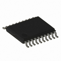
AT86RF401U-XI Atmel, AT86RF401U-XI Datasheet - Page 13

AT86RF401U-XI
Manufacturer Part Number
AT86RF401U-XI
Description
IC MICRO TX RF W/AVR 20-TSSOP
Manufacturer
Atmel
Datasheet
1.AT86RF401U-6GS.pdf
(52 pages)
Specifications of AT86RF401U-XI
Frequency
264MHz ~ 456MHz
Applications
Garage Opener, RKE, Telemetry
Modulation Or Protocol
ASK, OOK
Data Rate - Maximum
10 kbps
Power - Output
6dBm
Current - Transmitting
23.2mA
Data Interface
PCB, Surface Mount
Antenna Connector
PCB, Surface Mount
Memory Size
2KB Flash, 128 Byte EEPROM, 128Byte SRAM
Voltage - Supply
2 V ~ 5 V
Operating Temperature
-40°C ~ 85°C
Package / Case
20-TSSOP
Lead Free Status / RoHS Status
Contains lead / RoHS non-compliant
Features
-
Other names
AT86RF401U
Interrupt Response Time
Memory Programming
Program Memory Lock
Bits
In-system Flash and
EEPROM
SPI Interface
1424F–RKE–12/03
During power-on reset and watchdog reset, all I/O registers are set to their initial values,
and the program starts execution from address $000.
Note:
The interrupt execution response for all the enabled AVR interrupts is a minimum of four
clock cycles. After the four clock cycles, the program vector address for the actual inter-
rupt handling routine is executed. During this four clock cycle period, the Program
Counter is pushed onto the stack. The vector is a jump to the interrupt routine, and this
jump takes two clock cycles. If an interrupt occurs during execution of a multi-cycle
instruction, this instruction is completed before the interrupt is served.
A return from an interrupt handling routine takes four clock cycles. During these four
clock cycles, the Program Counter is popped back from the stack. When AVR exits from
an interrupt, it will always return to the main program and execute one more instruction
before any pending interrupt is served.
Note:
The AT86RF401 microtransmitter provides two lock bits that can be left unprogrammed
(“1”) or can be programmed (“0”) to obtain the additional features listed in Table 6.
Table 6. Lock Bit Protection Modes
Note:
The AT86RF401 offers 2 Kbytes (1K x 16) of in-system reprogrammable Flash program
memory and 128 bytes of EEPROM data memory. This memory can be programmed
serially via the SPI interface.
Both the program and data memory arrays can be programmed using the serial SPI bus
while RESETB is pulled to GND. The serial interface consists of pins SCK, SDI (input)
and SDO (output).
When programming, an auto-erase cycle is built into the self-timed programming opera-
tion, and there is no need to first execute the Chip Erase instruction. The Chip Erase
operation sets every memory location in the EEPROM array to $FF.
Either an external system clock is supplied at pin XTAL/CLK or a crystal needs to be
connected across pins XTAL/CLK and XTALB. The minimum low and high periods for
the serial clock (SCK) input are defined as follows:
Mod
Program Lock Bits
e
1
2
3
Low: 4 XTAL Clock Cycles
The instruction placed in address $000 must be an RJMP (relative jump) instruction or a
JMP (absolute jump) to the reset handling routine. If an RJMP or JMP instruction is not
present at address $000, the part is placed into a “no program” reset state. This is to pro-
tect the part from fetching instructions when no program is present.
The Status Register (SREG) is not saved by the AVR hardware. This must be performed
by user software when required.
The lock bits can only be erased with the Chip Erase operation.
LB1
1
0
0
LB2
1
1
0
Protection Type
No program lock features
Further serial (SPI) programming of the EEPROM is disabled (both
program and data memory).
Same as mode 2, but Verify is also disabled
High: 16 XTAL Clock Cycles
AT86RF401
13


