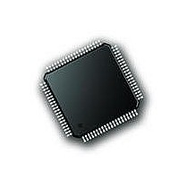
PIC18F86J72-I/PT Microchip Technology, PIC18F86J72-I/PT Datasheet - Page 174

PIC18F86J72-I/PT
Manufacturer Part Number
PIC18F86J72-I/PT
Description
IC PIC MCU 8BIT 14KB FLSH 80TQFP
Manufacturer
Microchip Technology
Series
PIC® 18Fr
Datasheet
1.PIC18F86J72-IPT.pdf
(480 pages)
Specifications of PIC18F86J72-I/PT
Program Memory Type
FLASH
Program Memory Size
64KB (32K x 16)
Package / Case
80-TQFP
Core Processor
PIC
Core Size
8-Bit
Speed
48MHz
Connectivity
I²C, LIN, SPI, UART/USART
Peripherals
Brown-out Detect/Reset, LCD, LVD, POR, PWM, WDT
Number Of I /o
51
Ram Size
3.8K x 8
Voltage - Supply (vcc/vdd)
2 V ~ 3.6 V
Data Converters
A/D 12x12b
Oscillator Type
Internal
Operating Temperature
-40°C ~ 85°C
Data Bus Width
8 bit
Data Ram Size
4 KB
Interface Type
SPI, USART, SPI, I2C
Maximum Clock Frequency
8 MHz
Number Of Programmable I/os
51
Number Of Timers
4
Operating Supply Voltage
2 V to 3.6 V
Maximum Operating Temperature
+ 85 C
Mounting Style
SMD/SMT
Minimum Operating Temperature
- 40 C
On-chip Adc
14
Controller Family/series
PIC18F
No. Of I/o's
51
Ram Memory Size
3923Byte
Cpu Speed
12MIPS
No. Of Timers
4
Rohs Compliant
Yes
Lead Free Status / RoHS Status
Lead free / RoHS Compliant
Lead Free Status / RoHS Status
Lead free / RoHS Compliant, Lead free / RoHS Compliant
Available stocks
Company
Part Number
Manufacturer
Quantity
Price
Company:
Part Number:
PIC18F86J72-I/PT
Manufacturer:
Microchip Technology
Quantity:
10 000
- Current page: 174 of 480
- Download datasheet (5Mb)
PIC18F87J72 FAMILY
17.3.3
PIC18F87J72 family devices have four distinct circuit
configurations for LCD bias generation:
• M0: Regulator with Boost
• M1: Regulator without Boost
• M2: Resistor Ladder with Software Contrast
• M3: Resistor Ladder with Hardware Contrast
17.3.3.1
In M0 operation, the LCD charge pump feature is
enabled. This allows the regulator to generate voltages
up to +3.6V to the LCD (as measured at LCDBIAS3).
M0 uses a flyback capacitor connected between
V
LCDBIAS0 through LCDBIAS3, to obtain the required
voltage boost (Figure 17-3). The output voltage (V
is the difference of potential between LCDBIAS3 and
LCDBIAS0. It is set by the BIAS<2:0> bits which adjust
the offset between LCDBIAS0 and V
capacitor (C
large LCD loads. This mode is useful in those cases
where the voltage requirements of the LCD are higher
than the microcontroller’s V
control of the display’s contrast by adjustment of bias
voltage by changing the value of the BIAS bits.
M0 supports Static and 1/3 Bias types. Generation of
the voltage levels for 1/3 Bias is handled automatically,
but must be configured in software.
M0 is enabled by selecting a valid regulator clock
source (CKSEL<1:0> set to any value except ‘00’) and
setting the CPEN bit. If Static Bias type is required, the
MODE13 bit must be cleared.
FIGURE 17-3:
DS39979A-page 174
LCAP
Note 1:
1 and V
BIAS CONFIGURATIONS
FLY
M0 (Regulator with Boost)
These values are provided for design guidance only. They should be optimized for the application by the designer based on the
actual LCD specifications.
LCAP
) acts as a charge storage element for
2, as well as filter capacitors on
LCD REGULATOR CONNECTIONS FOR M0 AND M1 CONFIGURATIONS
DD
PIC18F87J72
. It also permits software
LCDBIAS3
LCDBIAS2
LCDBIAS1
LCDBIAS0
V
V
SS
LCAP
LCAP
AV
. The flyback
DD
1
2
(V
V
BIAS
DD
BIAS
Mode 0
Preliminary
up to 3.6V)
)
C
0.47 µF
C3
0.47 µF
C2
0.47 µF
C1
0.47 µF
C0
0.47 µF
FLY
(1)
(1)
(1)
(1)
(1)
17.3.3.2
M1 operation is similar to M0, but does not use the LCD
charge pump. It can provide V
level supplied directly to LCDBIAS3. It can be used in
cases where V
never drop below a level that can provide adequate
contrast for the LCD. The connection of external com-
ponents is very similar to M0, except that LCDBIAS3
must be tied directly to V
The BIAS<2:0> bits can still be used to adjust contrast
in software by changing V
these bits changes the offset between LCDBIAS0 and
V
LCDBIAS0 and the voltage tied to LCDBIAS3. Thus, if
V
M0, the level of V
Like M0, M1 supports Static and 1/3 Bias types.
Generation of the voltage levels for 1/3 Bias is handled
automatically but must be configured in software.
M1 is enabled by selecting a valid regulator clock
source (CKSEL<1:0> set to any value except ‘00’) and
clearing the CPEN bit. If 1/3 Bias type is required, the
MODE13 bit should also be set.
SS
DD
Note:
. In M1, this is reflected in the change between the
should change, V
When the device enters Sleep mode while
operating in Bias modes, M0 or M1, be
sure that the bias capacitors are fully dis-
charged in order to get the lowest Sleep
current.
M1 (Regulator without Boost)
(V
DD
BIAS
Mode 1
BIAS
V
V
for the application is expected to
DD
DD
V
is constant.
C
0.47 µF
C2
0.47 µF
C1
0.47 µF
C0
0.47 µF
BIAS
DD
FLY
2010 Microchip Technology Inc.
DD
)
BIAS
will also change; where in
(Figure 17-3).
(1)
(1)
(1)
(1)
. As with M0, changing
BIAS
up to the voltage
Related parts for PIC18F86J72-I/PT
Image
Part Number
Description
Manufacturer
Datasheet
Request
R

Part Number:
Description:
Manufacturer:
Microchip Technology Inc.
Datasheet:

Part Number:
Description:
Manufacturer:
Microchip Technology Inc.
Datasheet:

Part Number:
Description:
Manufacturer:
Microchip Technology Inc.
Datasheet:

Part Number:
Description:
Manufacturer:
Microchip Technology Inc.
Datasheet:

Part Number:
Description:
Manufacturer:
Microchip Technology Inc.
Datasheet:

Part Number:
Description:
Manufacturer:
Microchip Technology Inc.
Datasheet:

Part Number:
Description:
Manufacturer:
Microchip Technology Inc.
Datasheet:

Part Number:
Description:
Manufacturer:
Microchip Technology Inc.
Datasheet:


