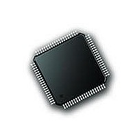
PIC18F86J72-I/PT Microchip Technology, PIC18F86J72-I/PT Datasheet - Page 458

PIC18F86J72-I/PT
Manufacturer Part Number
PIC18F86J72-I/PT
Description
IC PIC MCU 8BIT 14KB FLSH 80TQFP
Manufacturer
Microchip Technology
Series
PIC® 18Fr
Datasheet
1.PIC18F86J72-IPT.pdf
(480 pages)
Specifications of PIC18F86J72-I/PT
Program Memory Type
FLASH
Program Memory Size
64KB (32K x 16)
Package / Case
80-TQFP
Core Processor
PIC
Core Size
8-Bit
Speed
48MHz
Connectivity
I²C, LIN, SPI, UART/USART
Peripherals
Brown-out Detect/Reset, LCD, LVD, POR, PWM, WDT
Number Of I /o
51
Ram Size
3.8K x 8
Voltage - Supply (vcc/vdd)
2 V ~ 3.6 V
Data Converters
A/D 12x12b
Oscillator Type
Internal
Operating Temperature
-40°C ~ 85°C
Data Bus Width
8 bit
Data Ram Size
4 KB
Interface Type
SPI, USART, SPI, I2C
Maximum Clock Frequency
8 MHz
Number Of Programmable I/os
51
Number Of Timers
4
Operating Supply Voltage
2 V to 3.6 V
Maximum Operating Temperature
+ 85 C
Mounting Style
SMD/SMT
Minimum Operating Temperature
- 40 C
On-chip Adc
14
Controller Family/series
PIC18F
No. Of I/o's
51
Ram Memory Size
3923Byte
Cpu Speed
12MIPS
No. Of Timers
4
Rohs Compliant
Yes
Lead Free Status / RoHS Status
Lead free / RoHS Compliant
Lead Free Status / RoHS Status
Lead free / RoHS Compliant, Lead free / RoHS Compliant
Available stocks
Company
Part Number
Manufacturer
Quantity
Price
Company:
Part Number:
PIC18F86J72-I/PT
Manufacturer:
Microchip Technology
Quantity:
10 000
- Current page: 458 of 480
- Download datasheet (5Mb)
PIC18F87J72 FAMILY
B.6.2
The PHASE register (PHASE<7:0>) is a 7 bits + sign,
MSB first, two’s complement register that indicates how
much phase delay there should be between Channel 0
and Channel 1.
The reference channel for the delay is Channel 1
(typically, the voltage channel when used in energy
metering applications) i.e., when PHASE register code
is positive, Channel 0 is lagging Channel 1.
When PHASE register code is negative, Channel 0 is
leading versus Channel 1.
The delay is give by the following formula:
EQUATION B-17:
REGISTER B-2:
DS39979A-page 458
bit 7
Legend:
R = Readable bit
-n = Value at POR
bit 7-0
PHASE<7>
R/W-0
PHASE REGISTER
Delay
PHASE<7-0>: CH0 Relative to CH1 Phase Delay bits
Delay = PHASE register two’s complement code/DMCLK (Default PHASE = 0)
PHASE<6>
R/W-0
=
Phase Register Code
------------------------------------------------- -
PHASE: PHASE REGISTER (ADDRESS 0x07)
DMCLK
W = Writable bit
‘1’ = Bit is set
PHASE<5>
R/W-0
PHASE<4>
R/W-0
Preliminary
U = Unimplemented bit, read as ‘0’
‘0’ = Bit is cleared
PHASE<3>
R/W-0
B.6.2.1
The timing resolution of the phase delay is 1/DMCLK or
1 µs in the default configuration (MCLK = 4 MHz). The
PHASE register coding depends on the OSR setting,
as shown in Table B-15.
TABLE B-15:
Oversampling
<1:0>
OSR
00
01
10
11
Ratio
Value
PHASE<2>
128
256
32
64
Phase Resolution from OSR
R/W-0
PHASE ENCODING
RESOLUTION BY
OVERSAMPLING RATIO
Significant
7 <6:0>
6 <5:0>
5 <4:0>
4 <3:0>
Digits
2010 Microchip Technology Inc.
#
x = Bit is unknown
PHASE<1>
R/W-0
Encoding
Sign
<7>
<6>
<5>
<4>
Bit
PHASE<0>
-64 to +63
-32 to +31
-16 to +15
Range
-128 to
R/W-0
+127
bit 0
Related parts for PIC18F86J72-I/PT
Image
Part Number
Description
Manufacturer
Datasheet
Request
R

Part Number:
Description:
Manufacturer:
Microchip Technology Inc.
Datasheet:

Part Number:
Description:
Manufacturer:
Microchip Technology Inc.
Datasheet:

Part Number:
Description:
Manufacturer:
Microchip Technology Inc.
Datasheet:

Part Number:
Description:
Manufacturer:
Microchip Technology Inc.
Datasheet:

Part Number:
Description:
Manufacturer:
Microchip Technology Inc.
Datasheet:

Part Number:
Description:
Manufacturer:
Microchip Technology Inc.
Datasheet:

Part Number:
Description:
Manufacturer:
Microchip Technology Inc.
Datasheet:

Part Number:
Description:
Manufacturer:
Microchip Technology Inc.
Datasheet:


