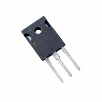
FCH47N60F_F133 Fairchild Semiconductor, FCH47N60F_F133 Datasheet - Page 2

FCH47N60F_F133
Manufacturer Part Number
FCH47N60F_F133
Description
MOSFET N-CH 600V 47A TO-247
Manufacturer
Fairchild Semiconductor
Series
SupreMOS™r
Datasheet
1.FCH47N60F_F133.pdf
(8 pages)
Specifications of FCH47N60F_F133
Fet Type
MOSFET N-Channel, Metal Oxide
Fet Feature
Standard
Rds On (max) @ Id, Vgs
73 mOhm @ 23.5A, 10V
Drain To Source Voltage (vdss)
600V
Current - Continuous Drain (id) @ 25° C
47A
Vgs(th) (max) @ Id
5V @ 250µA
Gate Charge (qg) @ Vgs
270nC @ 10V
Input Capacitance (ciss) @ Vds
8000pF @ 25V
Power - Max
417W
Mounting Type
Through Hole
Package / Case
TO-247-3
Lead Free Status / RoHS Status
Lead free / RoHS Compliant
Available stocks
Company
Part Number
Manufacturer
Quantity
Price
Part Number:
FCH47N60F_F133
Manufacturer:
FSC可看货
Quantity:
20 000
FCH47N60F _F133 Rev. A.
Package Marking and Ordering Information
Electrical Characteristics
NOTES:
1. Repetitive Rating: Pulse width limited by maximum junction temperature
2. I
3. I
4. Pulse Test: Pulse width ≤ 300μs, Duty Cycle ≤ 2%
5. Essentially Independent of Operating Temperature Typical Characteristics
Off Characteristics
BV
ΔBV
/
BV
I
I
I
On Characteristics
V
R
g
Dynamic Characteristics
C
C
C
C
C
Switching Characteristics
t
t
t
t
Q
Q
Q
Drain-Source Diode Characteristics and Maximum Ratings
I
I
V
t
Q
Device Marking
Symbol
DSS
GSSF
GSSR
d(on)
r
d(off)
f
S
SM
rr
FS
GS(th)
SD
AS
SD
DS(on)
iss
oss
rss
oss
oss
g
gs
gd
rr
DSS
DS
ΔT
= 18A, V
≤ 47A, di/dt ≤ 1,200A/μs, V
FCH47N60F
DSS
eff.
J
DD
Drain-Source Breakdown Voltage
Breakdown Voltage Temperature
Coefficient
Drain-Source Avalanche Breakdown
Voltage
Zero Gate Voltage Drain Current
Gate-Body Leakage Current, Forward
Gate-Body Leakage Current, Reverse
Gate Threshold Voltage
Static Drain-Source
On-Resistance
Forward Transconductance
Input Capacitance
Output Capacitance
Reverse Transfer Capacitance
Output Capacitance
Effective Output Capacitance
Turn-On Delay Time
Turn-On Rise Time
Turn-Off Delay Time
Turn-Off Fall Time
Total Gate Charge
Gate-Source Charge
Gate-Drain Charge
Maximum Continuous Drain-Source Diode Forward Current
Maximum Pulsed Drain-Source Diode Forward Current
Drain-Source Diode Forward Voltage
Reverse Recovery Time
Reverse Recovery Charge
= 50V, R
G
= 25Ω, Starting T
FCH47N60F_F133
DD
Parameter
≤ BV
Device
DSS
, Starting T
J
= 25°C
J
T
= 25°C
C
= 25°C unless otherwise noted
Package
TO-247
V
V
V
V
V
V
V
I
V
V
V
V
V
V
f = 1.0MHz
V
V
V
R
V
V
dI
D
GS
GS
GS
DS
DS
GS
GS
DS
GS
DS
DS
DS
DS
DD
G
DS
GS
GS
GS
F
= 250μA, Referenced to 25°C
/dt =100A/μs
= 25Ω
= 600V, V
= 480V, T
= V
= 40V, I
= 25V, V
= 480V, V
= 0V to 400V, V
= 480V, I
= 0V, I
= 0V, I
= 0V, I
= 30V, V
= -30V, V
= 10V, I
= 300V, I
= 10V
= 0V, I
= 0V, I
GS
2
, I
D
D
D
S
S
D
D
D
Conditions
= 250μA, T
= 250μA, T
= 47A
= 47A
= 47A
GS
DS
D
D
DS
C
= 23.5A
= 23.5A
GS
= 250μA
GS
= 47A
= 47A
Reel Size
= 125°C
= 0V
= 0V,
= 0V
= 0V
= 0V, f = 1.0MHz
GS
-
= 0V
J
J
= 25°C
= 150°C
(Note 4, 5)
(Note 4, 5)
(Note 4)
(Note 4)
Tape Width
Min
600
-
3.0
--
--
--
--
--
--
--
--
--
--
--
--
--
--
--
--
--
--
--
--
--
--
--
--
--
--
0.062
5900
3200
Typ
2.04
250
650
700
160
420
185
210
520
210
110
240
0.6
40
75
38
--
--
--
--
--
--
--
--
--
Quantity
0.073
Max Units
8000
4200
1100
-100
www.fairchildsemi.com
100
100
430
450
160
270
141
5.0
1.4
10
47
--
--
--
--
--
--
--
--
--
--
--
--
30
V/°C
μA
μA
nA
nA
nC
nC
nC
μC
pF
pF
pF
pF
pF
ns
ns
ns
ns
ns
Ω
V
V
V
V
S
A
A
V


