VNC2-48Q1B-REEL FTDI, VNC2-48Q1B-REEL Datasheet - Page 25
VNC2-48Q1B-REEL
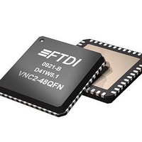
Manufacturer Part Number
VNC2-48Q1B-REEL
Description
USB Interface IC Vinculum-II Dual USB Host/Dev IC QFN-48
Manufacturer
FTDI
Type
USB Host/Device Controllerr
Datasheet
1.VNC2-32Q1B-REEL.pdf
(90 pages)
Specifications of VNC2-48Q1B-REEL
Maximum Operating Temperature
+ 85 C
Minimum Operating Temperature
- 40 C
Mounting Style
SMD/SMT
Operating Temperature Range
- 40 C to + 85 C
Supply Current
25 mA
Operating Supply Voltage
1.8 V, 3.3V
Package / Case
QFN-48
Description/function
USB Vinculum-II Dual Host/Dev IC QFN-48
Lead Free Status / RoHS Status
Lead free / RoHS Compliant
Other names
VINCULUM2


4.2.5 Peripheral DMA Modules 0, 1, 2 & 3
The peripheral DMA has the capability to transfer data to and from an I/O device. The CPU can offload
the transfer of data between the processor and the peripheral freeing the CPU to execute other
instructions.
The DMA module collects or transmits data from memory to an I/O address space, it is also capable of
copying data in memory and transferring it to another location.
The DMA is not accessible by the user as it automatically controlled by the CPU.
4.2.6 RAM Module
The RAM module consists of 16k bytes on-chip (4k x 32-bits) data memory. The RAM is byte addressable.
4.2.7 Peripheral Interface Modules
VNC2 has nine peripheral interface modules. Full descriptions of each module are described in section 6.
4.2.8 USB Transceivers 0 and 1
Two USB transceiver cells provide the physical USB device interface supporting USB 1.1 and USB 2.0
standards. Low-speed and full-speed USB data rates are supported. Each output driver provides +3.3V
level slew rate control signalling, whilst a differential receiver and two single ended receivers provide USB
DATA IN, SE0 and USB Reset condition detection. These cells also include integrated internal USB pull-up
or pull-down resistors as required for host or slave mode.
4.2.9 USB Host / Device Controllers
These blocks handle the parallel-to-serial and serial-to-parallel conversion of the USB physical layer. This
includes bit stuffing, CRC generation, USB frame generation and protocol error checking. The Host /
Device controller is autonomous and therefore requires limited load from the CPU.
4.2.10 12MHz Oscillator
The 12MHz Oscillator cell generates a 12MHz reference clock input to the Clock Multiplier PLL from an
external 12MHz crystal. The external crystal is connected across Pin 4 – XTIN and Pin 5 – XTOUT in the
configuration shown in Figure 10-1.
4.2.11 Power Saving Modes and Standby mode.
VNC2 can be set to operate in three frequencies allowing the user to select a slower speed to reduce
power consumption. Three operating frequencies available are 12MHz, 24MHz and normal operation of
48MHz. These operating modes can be configured using the RTOS. Full details are available in the RTOS
manual available from the
When a particular peripheral is not used, it is powered down internally thus saving power.
Standby mode is available under firmware control, this mode puts the VNC2 in a state with no clocks
running or system blocks powered. The device will wake up out of this mode by toggling any of the
following signals: USB0/1 DP or DM, SPI slave 0 select (spi_s0_ss# ), SPI slave 1select(spi_s1_ss#
UART ring indicator (uart_ri#).
Debugger Interface
UART
PWM
FIFO
SPI Master
SPI Slave 0 & 1
GPIO - General purpose I/O pins
General purpose timers
Copyright © 2010 Future Technology Devices International Limited
FTDI
VINCULUM-II EMBEDDED DUAL USB HOST CONTROLLER IC Datasheet
website.
Document No.: FT_000138
Clearance No.: FTDI#
Version -
)
143
1.2
or
25
Related parts for VNC2-48Q1B-REEL
Image
Part Number
Description
Manufacturer
Datasheet
Request
R

Part Number:
Description:
Interface Modules & Development Tools USB to Serial UART MiniB Dev Mod FT232R
Manufacturer:
FTDI
Datasheet:

Part Number:
Description:
BOARD, EVALUATION, EU PSU
Manufacturer:
FTDI
Datasheet:
Part Number:
Description:
BOARD, EVALUATION, UK PSU
Manufacturer:
FTDI
Datasheet:
Part Number:
Description:
BOARD, EVALUATION, US PSU
Manufacturer:
FTDI
Datasheet:
Part Number:
Description:
Specifications: Manufacturer: FTDI ; Product Category: USB Interface IC ; RoHS: Details ; Operating Supply Voltage: 3 V to 5.25 V ; Supply Current: 25 mA ; Maximum Operating Temperature: + 70 C ; Mounting Style: SMD/SMT ; Package / Case: QFN-32
Manufacturer:
FTDI
Part Number:
Description:
integr. usb2.0/uart lqfp32 rohs ftdi reel c1k...
Manufacturer:
FTDI
Datasheet:
Part Number:
Description:
Interface Development Tools USB to UART Breakout Board
Manufacturer:
FTDI
Datasheet:

Part Number:
Description:
IC USB TO SERIAL UART 32-QFN
Manufacturer:
FTDI, Future Technology Devices International Ltd

Part Number:
Description:
USB Interface IC USB to Serial UART Enhanced IC SSOP-28
Manufacturer:
FTDI
Datasheet:

Part Number:
Description:
IC, USB UART INTERFACE, SSOP-28
Manufacturer:
FTDI
Datasheet:

Part Number:
Description:
IC, USB UART INTERFACE, QFN-32
Manufacturer:
FTDI
Datasheet:
Part Number:
Description:
IC, USB FIFO INTERFACE, SSOP-28
Manufacturer:
FTDI
Datasheet:
Part Number:
Description:
MODULE, USB, 4 PORT, FT4232H BASED
Manufacturer:
FTDI
Datasheet:
Part Number:
Description:
357-036-542-201 CARDEDGE 36POS DL .156 BLK LOPRO
Manufacturer:
FTDI
Datasheet:
Part Number:
Description:
357-036-542-201 CARDEDGE 36POS DL .156 BLK LOPRO
Manufacturer:
FTDI
Datasheet: