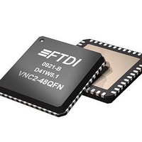
VNC2-48Q1B-REEL FTDI, VNC2-48Q1B-REEL Datasheet - Page 26

VNC2-48Q1B-REEL
Manufacturer Part Number
VNC2-48Q1B-REEL
Description
USB Interface IC Vinculum-II Dual USB Host/Dev IC QFN-48
Manufacturer
FTDI
Type
USB Host/Device Controllerr
Datasheet
1.VNC2-32Q1B-REEL.pdf
(90 pages)
Specifications of VNC2-48Q1B-REEL
Maximum Operating Temperature
+ 85 C
Minimum Operating Temperature
- 40 C
Mounting Style
SMD/SMT
Operating Temperature Range
- 40 C to + 85 C
Supply Current
25 mA
Operating Supply Voltage
1.8 V, 3.3V
Package / Case
QFN-48
Description/function
USB Vinculum-II Dual Host/Dev IC QFN-48
Lead Free Status / RoHS Status
Lead free / RoHS Compliant
Other names
VINCULUM2
5
FTDI devices typically have multiple interfaces available to communicate with external devices. VNC2 has
UART, SPI slave0, SPI slave1, SPI master, FIFO, GPIO, and PWM peripherals. The available packages for
VNC2 provide any of these interfaces to be active on the available pins through the use of an I/O
Multiplexer. Table 8 lists the signals available for each peripheral. Table 9 to 12 explain the use of the
I/O multiplexer.
Multiplexers are used to connect the VNC2 peripherals to the external IOBUS pins. This enables the
designer to select which IOBUS pins he wishes to map a particular peripheral to. Peripheral signals are
allocated to one of four groups, which connect to the I/O multiplexer. Each I/O peripheral signal can
connect to one out of every four external IOBUS pins. The IOBUS pin that a peripheral signal can connect
to is dictated by the peripheral signal‟s group. For example, if a peripheral signal is allocated to group 0
then it can connect to IOBUS0, IOBUS4, IOBUS8, IOBUS12 and so on. If a peripheral signal is allocated
to group 1 then it can connect to IOBUS1, IOBUS5, IOBUS9, IOBUS13 and so on. Figure 5-1 details the
I/O multiplexer concept, where, for example, a white peripheral signal can connect to any white IOBUS
pin, a green peripheral signal can connect to a green IOBUS pin. Figure 5-2, Figure 5-3 and Figure 5-4
give examples of connecting peripheral signals to differing IOBUS pins.
The IO Multiplexer also provides the following features:
Note: It is recommended not to reassign the debug interface signal (debug_if) from its default
setting of IOBUS0 (Pin 11 on all packages). This assumes that the debug pin is required in the
application design, if not, pin 11 can be assigned to any other group 0 signal.
An application (IOMUX) within the RTOS is available to aid with pin configuration, Section 5.2 has more
details.
Further details of the IO Multiplexer are available within Application Note AN_139
Explained.
I/O Multiplexer
Ability to configure an I/O pad as an input, output or bidirectional pad.
At power on reset, all pins are set as inputs by default. Whenever the I/O Mux is enabled the pins
are configured as their default values listed Table 6 within section 3.12.
Copyright © 2010 Future Technology Devices International Limited
VINCULUM-II EMBEDDED DUAL USB HOST CONTROLLER IC Datasheet
Document No.: FT_000138
Clearance No.: FTDI#
Vinculum-II IO Mux
Version -
143
1.2
26


